25)
A transistor collector characteristic curve is a graph showing
25)
A)
collector current (IC) versus collector–emitter voltage (VCE) for specified values of base
current (IB).
B)
collector current (IC) versus collector–emitter voltage (VCC) for specified values of base
current
(IB).
C)
collector current (IC) versus collector–emitter voltage (VC) for specified values of base current
(IB).
D)
emitter current (IE) versus collector–emitter voltage (VCE) for specified values of base current
(IB).
Answer:
A
Explanation:
A)
B)
C)
D)
26)
A BJT has an IB of 75 µA and a dc of 100. The value of IC is
26)
A)
75 mA.
B)
7.5 mA.
C)
10 mA.
D)
175 µA.
Answer:
B
Explanation:
A)
B)
C)
D)
27)
In an NPN transistor, the majority carriers in the base are
27)
A)
free electrons.
B)
holes.
C)
Neither A nor B.
D)
Both A and B.
Answer:
B
Explanation:
A)
B)
C)
D)
28)
The signal output voltage (Vout) is a function of the
28)
A)
changing collector current (IC) through the collector resistor RC.
B)
voltage drop from base to collector.
C)
power being dissipated by the base supply voltage.
D)
current from base to collector.
Answer:
A
Explanation:
A)
B)
C)
D)
8
29)
A 35 mV signal is applied to the base of a properly biased transistor with an r‘ e= 8 and RC= 1 k
. The output signal voltage at the collector is
29)
A)
28.57 V.
B)
3.5 V.
C)
4.375 V.
D)
4.375 mV.
Answer:
C
Explanation:
A)
B)
C)
D)
30)
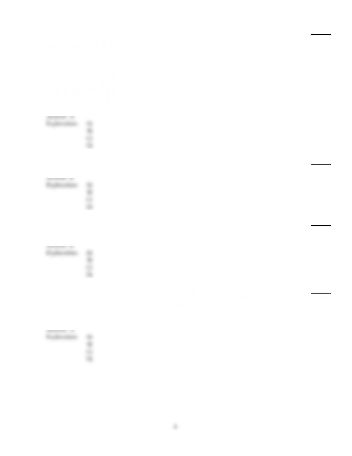
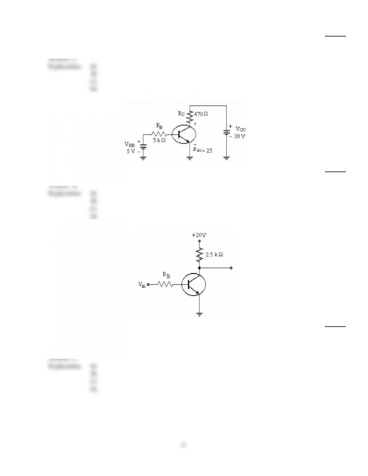
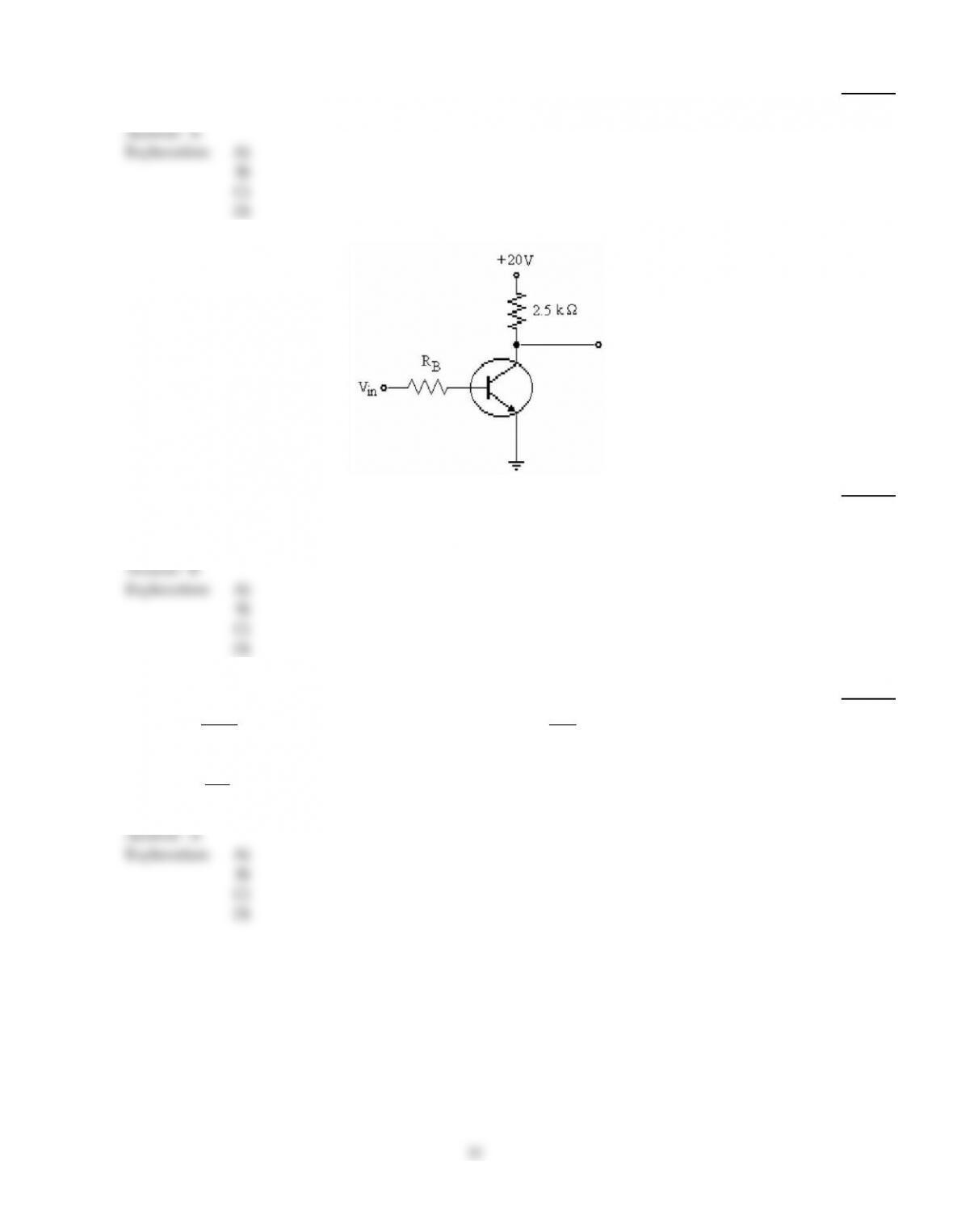
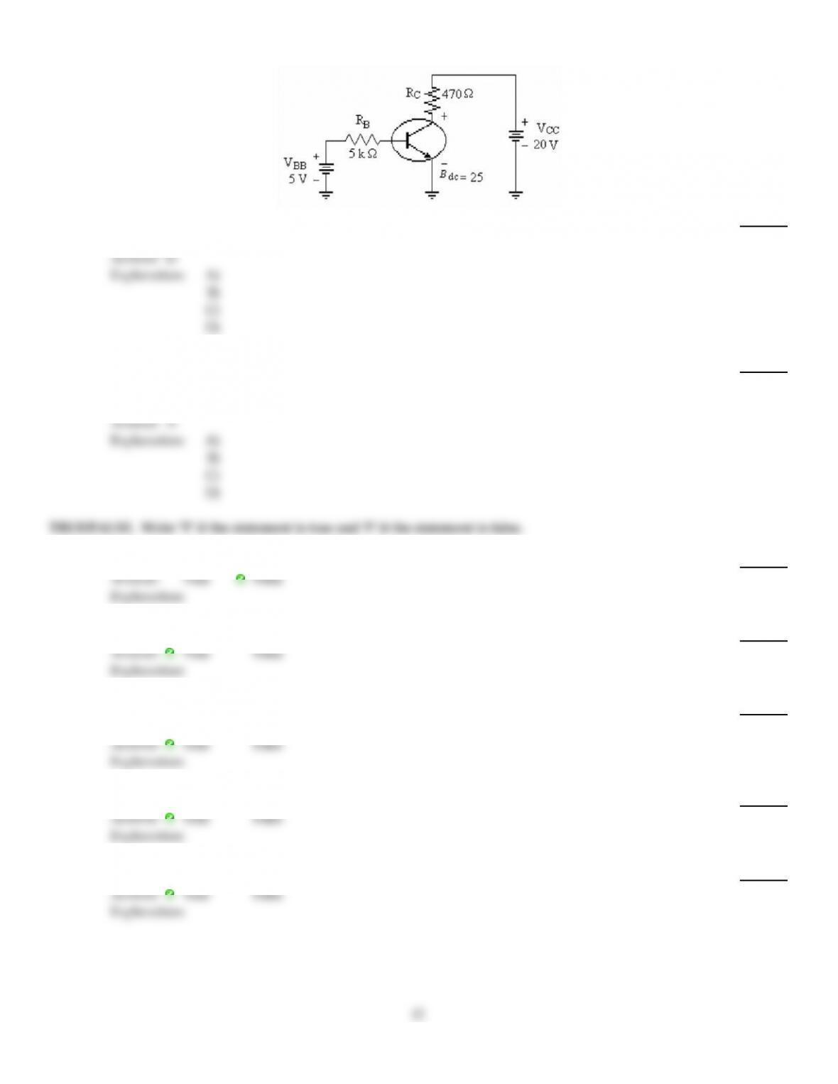
Refer to the figure above. If this transistor is operating in saturation, the value of IC(sat) is
30)
A)
9.4 mA.
B)
42.6 mA.
C)
28.6 mA.
D)
4.26 mA.
Answer:
B
Explanation:
A)
B)
C)
D)
31)
Refer to the figure above. This circuit is saturated. To get the circuit to operate close to its linear
range
31)
A)
Vin should be increased.
B)
RC should be decreased.
C)
RB should be increased.
D)
RB should be decreased.
Answer:
C
Explanation:
A)
B)
C)
D)
9
32)
Refer to the figure above. The voltage VCE was measured and found to be 20 V. The transistor is
operating in
32)
A)
the active region.
B)
saturation.
C)
cutoff.
D)
Not enough data to determine.
Answer:
C
Explanation:
A)
B)
C)
D)
33)
When a transistor switch is on, the collector current is limited by
33)
A)
the base current.
B)
the base voltage.
C)
the collector resistance.
D)
the base resistance.
Answer:
C
Explanation:
A)
B)
C)
D)
34)
A transistor amplifier has an input voltage of 67 mV and an output voltage of 2..48 V. The voltage
gain is
34)
A)
27.
B)
67.
C)
17.
D)
37.
Answer:
D
Explanation:
A)
B)
C)
D)
35)
Refer to the figure above. If the value of VBB were increased to 10 V, the transistor would be
operating in
35)
A)
the active region.
B)
cutoff.
C)
saturation.
D)
Cannot be determined.
Answer:
C
Explanation:
A)
B)
C)
D)
10
36)
A transistor has a DC of 250 and a base current, IB, of 20 µA. The collector current, IC, equals
36)
A)
5 mA.
B)
500 µA.
C)
5 A.
D)
50 mA.
Answer:
A
Explanation:
A)
B)
C)
D)
37)
Refer to the figure above. If the measured voltage from the collector to ground were 0 V, the
transistor is operating in
37)
A)
the active region.
B)
saturation.
C)
cutoff.
D)
Not enough data to determine.
Answer:
B
Explanation:
A)
B)
C)
D)
38)
The signal voltage gain of an amplifier, AV, is defined as
38)
A)
AV=Vout
Vin .
B)
AV=Rc
RL.
C)
AV=r’ e
RC.
D)
AV=IB x RB.
Answer:
A
Explanation:
A)
B)
C)
D)
11
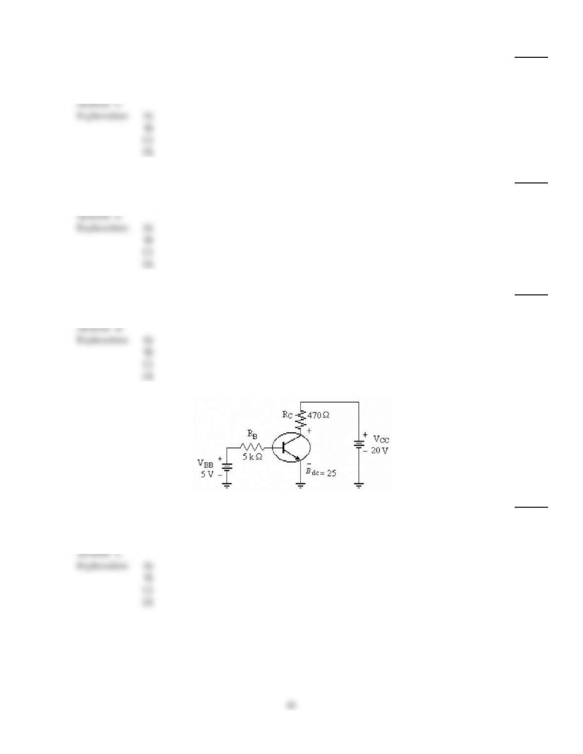
39)
Refer to the figure above. The value of IB is
39)
A)
1 mA.
B)
8.6 mA.
C)
0.7 µA.
D)
860 µA.
Answer:
D
Explanation:
A)
B)
C)
D)
40)
A 22 mV signal is applied to the base of a properly biased transistor that has an r’ e= 7 and an RC
= 1.2 k. The output voltage at the collector is
40)
A)
3.77 V.
B)
7 V.
C)
22 mV.
D)
17.1 V.
Answer:
A
Explanation:
A)
B)
C)
D)
TRUE/FALSE. Write ‘T’ if the statement is true and ‘F’ if the statement is false.
41)
A BJT transistor has the base–emitter junction reverse–biased for proper operation.
41)
Answer:
True
False
Explanation:
42)
Proper operation of a BJT requires that the base–collector junction should be reverse–biased.
42)
Answer:
True
False
Explanation:
43)
When a transistor is checked out–of–circuit, a very low resistance reading should be obtained
between the C and E leads of a good transistor.
43)
Answer:
True
False
Explanation:
44)
BJT transistors have two pn junctions.
44)
Answer:
True
False
Explanation:
45)
The formula for IC is IC= IE– IB.
45)
Answer:
True
False
Explanation:
12

46)
Phototransistors come in both two and three terminal configurations.
46)
Answer:
True
False
Explanation:
47)
The ratio IE/IC is dc.
47)
Answer:
True
False
Explanation:
13