Exam
Name___________________________________
MULTIPLE CHOICE. Choose the one alternative that best completes the statement or answers the question.
1)
When transistors are used in digital circuits they usually operate in the
1)
A)
linear region.
B)
saturation and cutoff regions.
C)
active region.
D)
breakdown region.
Answer:
B
Explanation:
A)
B)
C)
D)
2)
Normal operation of an NPN BJT requires the base to be ________ with respect to the emitter, and
________ with respect to the collector.
2)
A)
negative, positive
B)
positive, negative
C)
negative, negative
D)
positive, positive
Answer:
B
Explanation:
A)
B)
C)
D)
3)
If the collector resistance in a transistor amplifier is open, the dc voltage at the collector will be
closest to
3)
A)
VCC.
B)
VCC/2.
C)
0 V.
D)
VBB.
Answer:
C
Explanation:
A)
B)
C)
D)
4)
Besides operating as an amplifier, the BJT is often applied as a
4)
A)
variable inductor.
B)
switch.
C)
varactor.
D)
voltage controlled capacitance.
Answer:
B
Explanation:
A)
B)
C)
D)
5)
A certain transistor has an IC= 12 mA and an IB= 125 µA. dc is
5)
A)
96.
B)
12.
C)
15.
D)
150.
Answer:
A
Explanation:
A)
B)
C)
D)
1
6)
In a transistor, the relation of the three transistor currents is
6)
A)
IE= IC+ IB.
B)
IC= IE+ IB.
C)
IC= IE+VC/RC.
D)
IC= IB– 2IE.
Answer:
A
Explanation:
A)
B)
C)
D)
7)
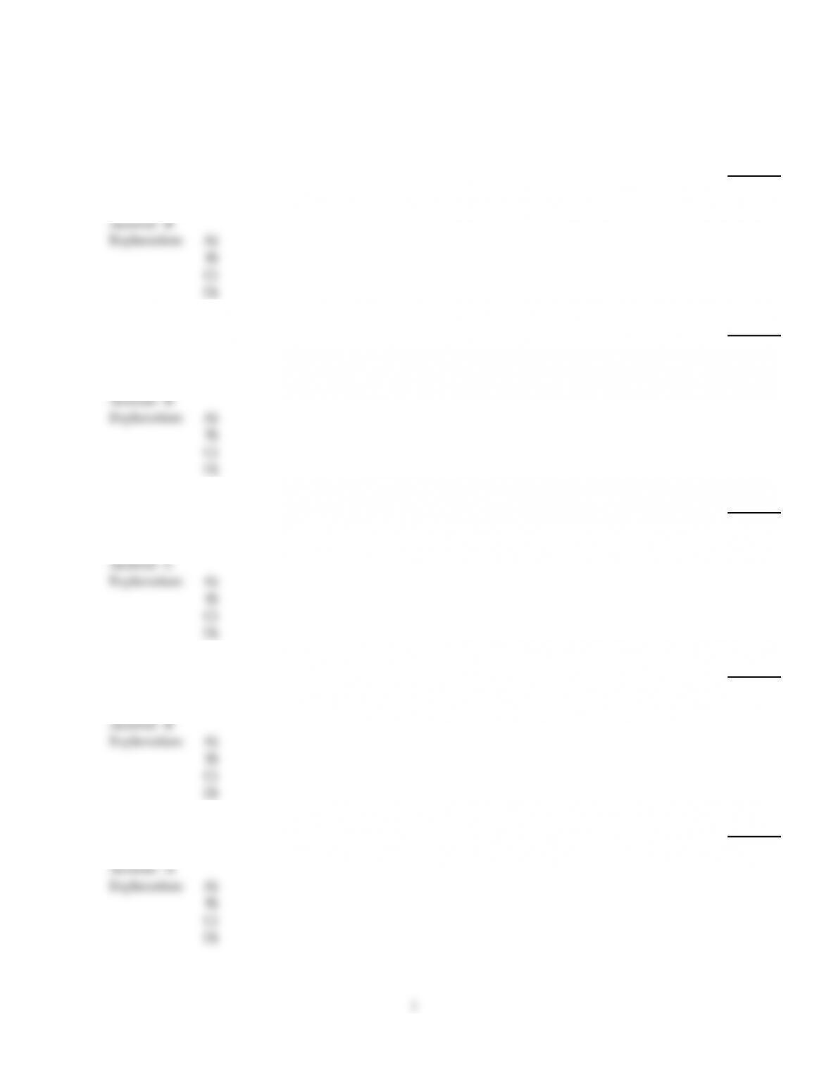
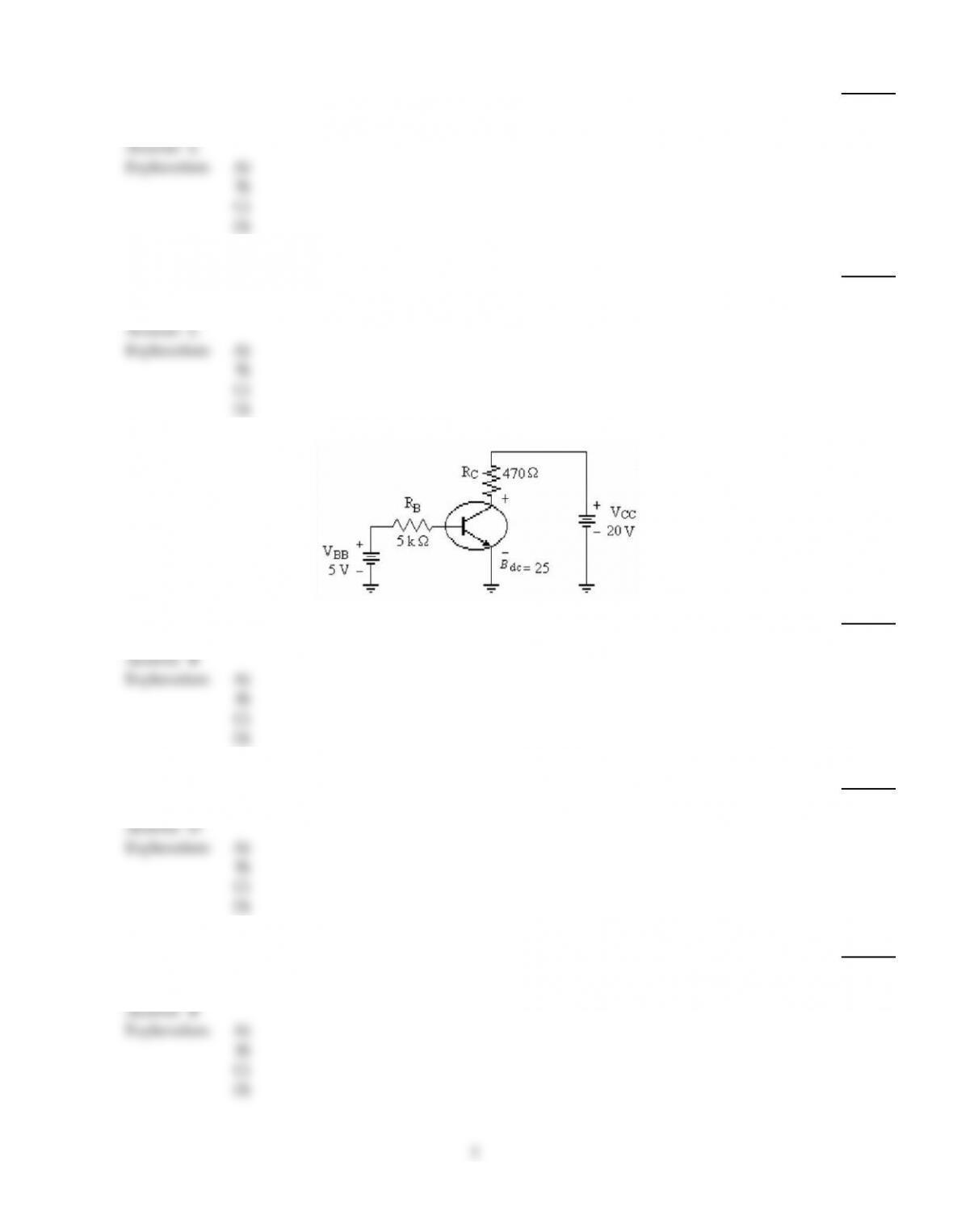
Refer to the figure above. If VCE is measured and is equal to nearly zero, the transistor is operating
in
7)
A)
cutoff.
B)
saturation.
C)
the active region.
D)
Cannot be determined.
Answer:
B
Explanation:
A)
B)
C)
D)
2
8)
Refer to the figure above. Assume that this circuit is operating in cutoff. The measurement, if any,
that would confirm this assumption is
8)
A)
VCE = 8 V.
B)
VCE = 20 V.
C)
VCC = 20 V.
D)
VBE = 0.7 V.
E)
None of the above.
Answer:
B
Explanation:
A)
B)
C)
D)
E)
9)
The base–to–emitter junction of a certain transistor is checked with a DMM on diode check in the
forward bias direction. If the DMM indicates 0.700, the transistor is
9)
A)
silicon and measuring normal.
B)
germanium and measuring normal.
C)
open between the base and emitter.
D)
definitely defective.
Answer:
A
Explanation:
A)
B)
C)
D)
3
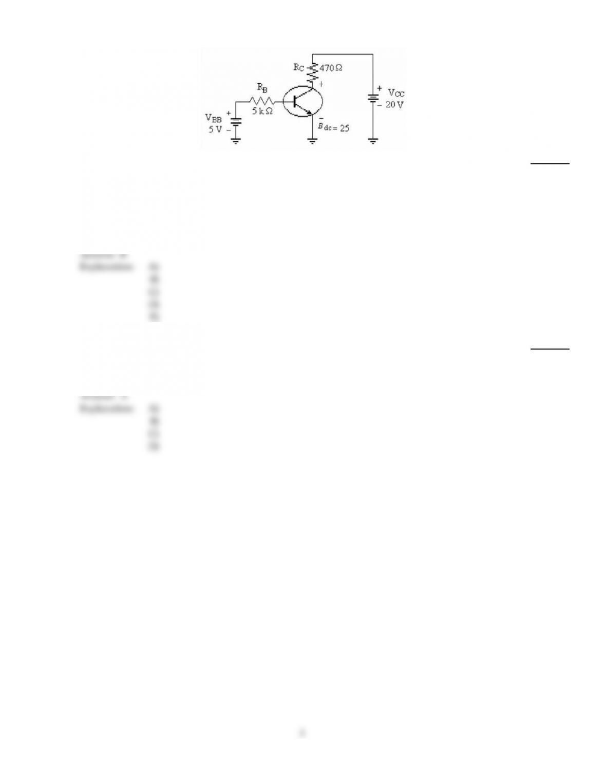
10)
Refer to the figure above. If the collector resistor value is changed to 4.7 k and dc = 200, IC(sat)
would
be
10)
A)
4.26 µA.
B)
8 mA.
C)
8.426 mA.
D)
4.26 mA.
Answer:
D
Explanation:
A)
B)
C)
D)
11)
Refer to the figure above. The value of IC at cutoff is
11)
A)
0 mA.
B)
10.65 µA.
C)
10 mA.
D)
2.13 mA.
Answer:
A
Explanation:
A)
B)
C)
D)
12)
An open base resistor (RB) in a transistor switch will result in the
12)
A)
transistor being instantly destroyed.
B)
transistor always being OFF.
C)
transistor operating in the active region.
D)
transistor always being ON.
Answer:
B
Explanation:
A)
B)
C)
D)
4
13)
In a bipolar junction transistor, collector current is controlled by
13)
A)
collector resistance.
B)
collector voltage.
C)
base current.
D)
All of the above.
Answer:
C
Explanation:
A)
B)
C)
D)
14)
Most of the electrons in the base of an NPN transistor flow
14)
A)
out of the base lead.
B)
into the base supply.
C)
into the collector.
D)
into the emitter.
Answer:
C
Explanation:
A)
B)
C)
D)
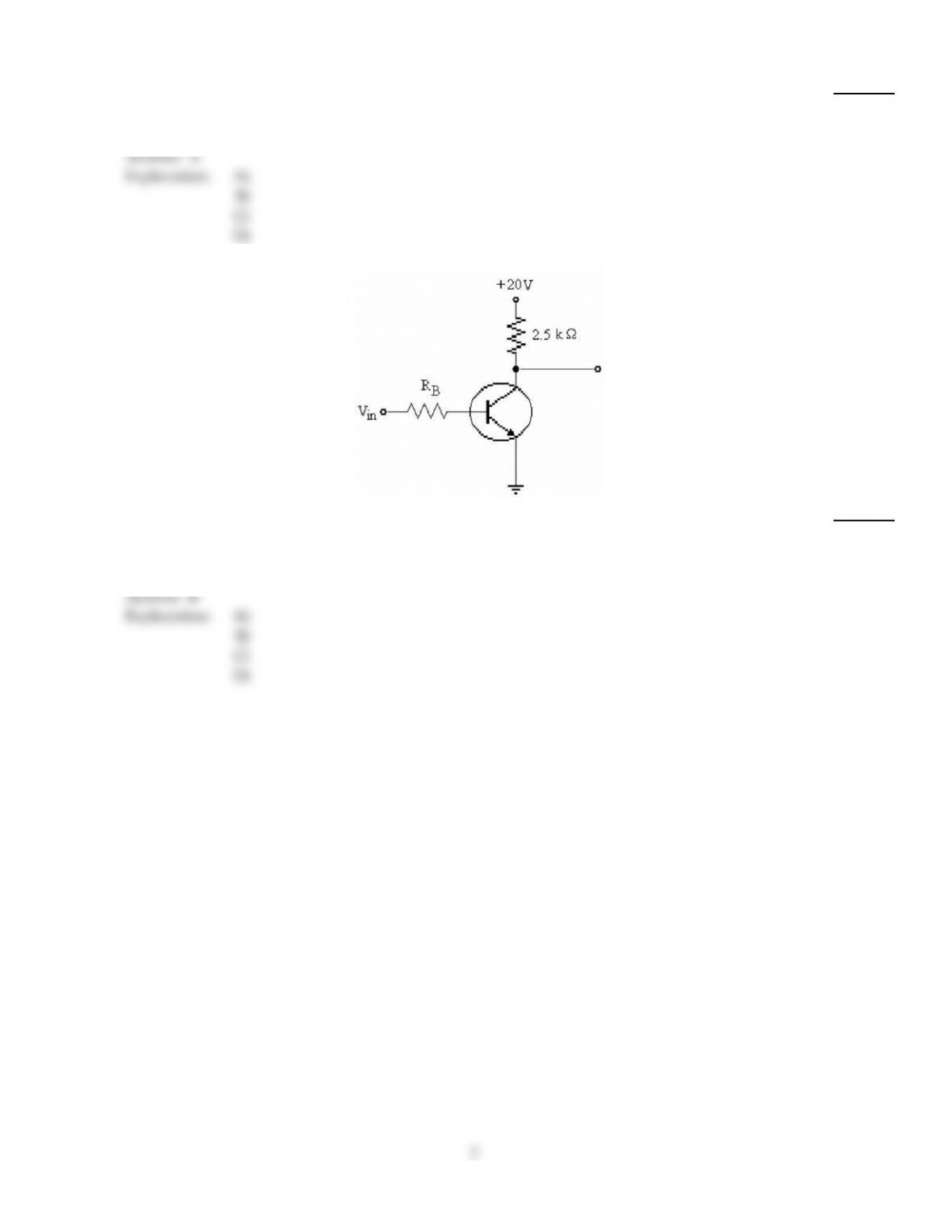
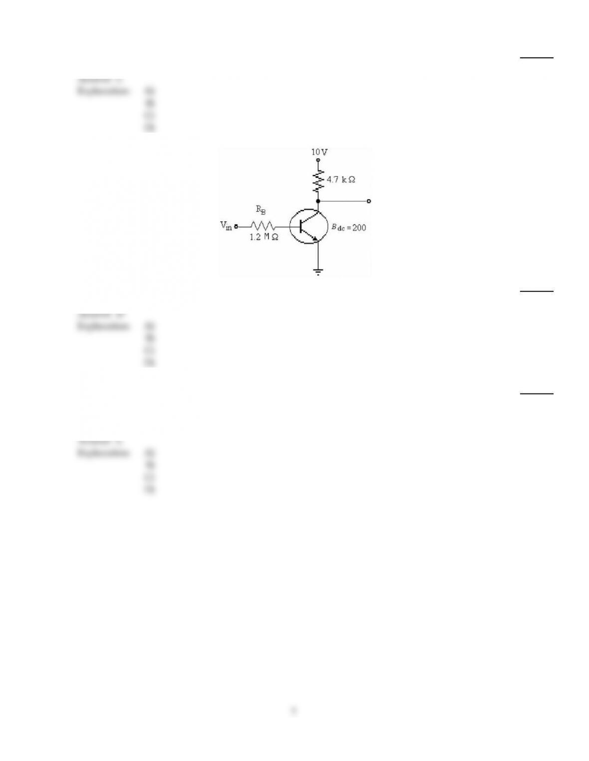
15)
Refer to the figure above. The value of VCE is
15)
A)
19.3 V.
B)
9.9 V.
C)
9.2 V.
D)
0.7 V.
Answer:
B
Explanation:
A)
B)
C)
D)
16)
VCE approximately equals ________ when a transistor switch is in saturation.
16)
A)
VC
B)
VB
C)
0.7 V
D)
0.2 V
Answer:
D
Explanation:
A)
B)
C)
D)
17)
The base of an NPN transistor is thin and
17)
A)
metallic.
B)
lightly doped.
C)
heavily doped.
D)
doped by a pentavalent material.
Answer:
B
Explanation:
A)
B)
C)
D)
5
18)
Refer to the figure above. This circuit is operating
18)
A)
in cutoff.
B)
incorrectly because the bias voltages are wrong.
C)
in saturation.
D)
in the active region.
Answer:
D
Explanation:
A)
B)
C)
D)
19)
When a transistor is operated in the active region, changes in the collector supply voltage VCC
19)
A)
produce changes in base voltage.
B)
have little or no effect on collector current.
C)
produce changes in collector current.
D)
produce changes in emitter voltage.
Answer:
B
Explanation:
A)
B)
C)
D)
20)
The symbol hFE is the same as
20)
A)
DC.
B)
hj–fj.
C)
ac.
D)
DC.
Answer:
A
Explanation:
A)
B)
C)
D)
21)
The region in a transistor that has to dissipate the most heat is the
21)
A)
anode.
B)
emitter.
C)
base.
D)
collector.
Answer:
D
Explanation:
A)
B)
C)
D)
6
22)
A bipolar junction transistor has ________ regions of operation.
22)
A)
1
B)
2
C)
3
D)
4
Answer:
C
Explanation:
A)
B)
C)
D)
23)
Refer to the figure above. The minimum value of IB that will produce saturation is
23)
A)
0.25 mA.
B)
1.064 µA
C)
5.325 µA.
D)
10.64 µA
Answer:
D
Explanation:
A)
B)
C)
D)
24)
Refer to the figure above. If the value of the collector resistor is increased to 6.8 k, the new value
of
IC(sat) is
24)
A)
2.13 mA.
B)
0 mA.
C)
1.47 mA.
D)
0.68 mA.
Answer:
C
Explanation:
A)
B)
C)
D)
7