Exam
Name___________________________________
MULTIPLE CHOICE. Choose the one alternative that best completes the statement or answers the question.
1)
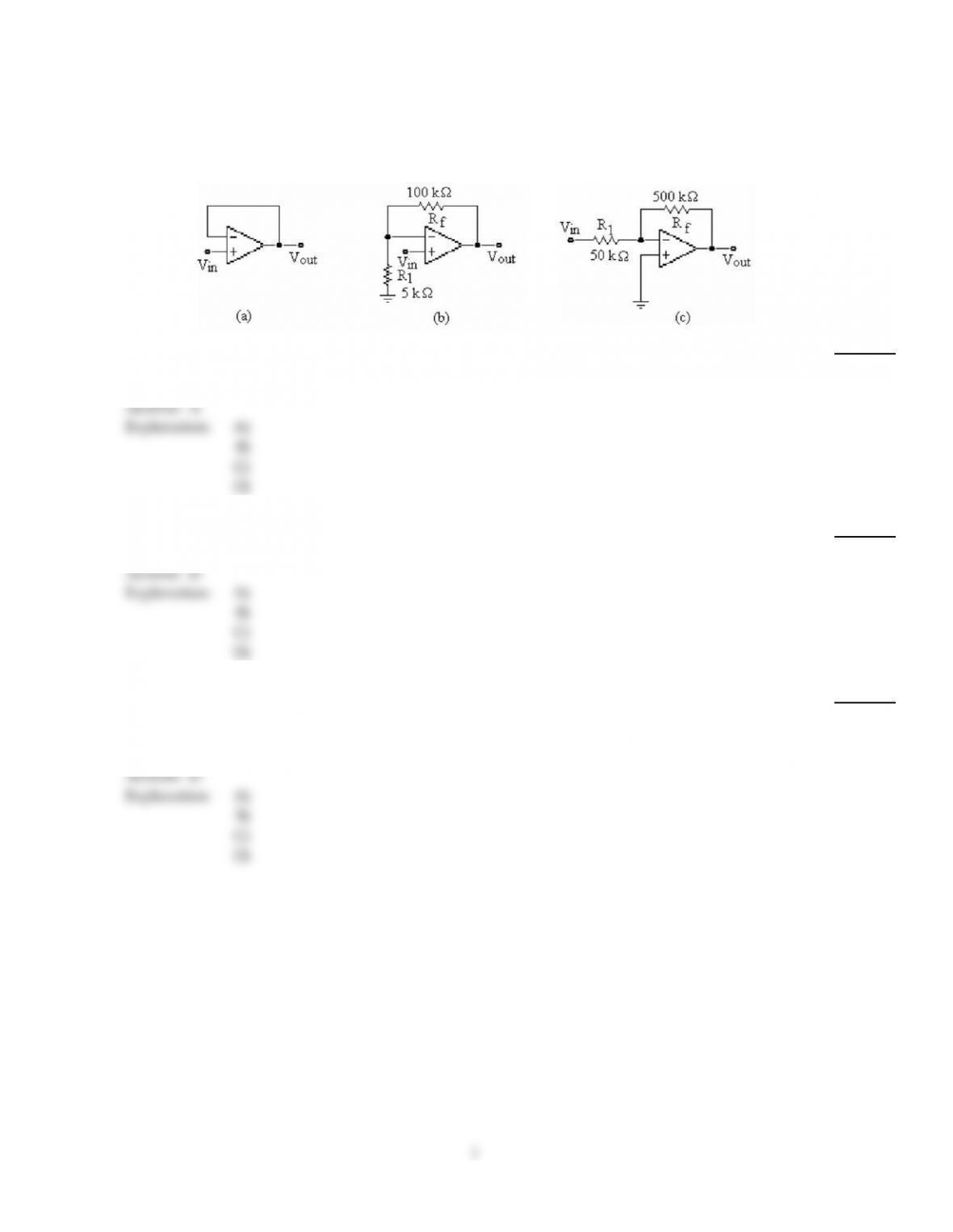
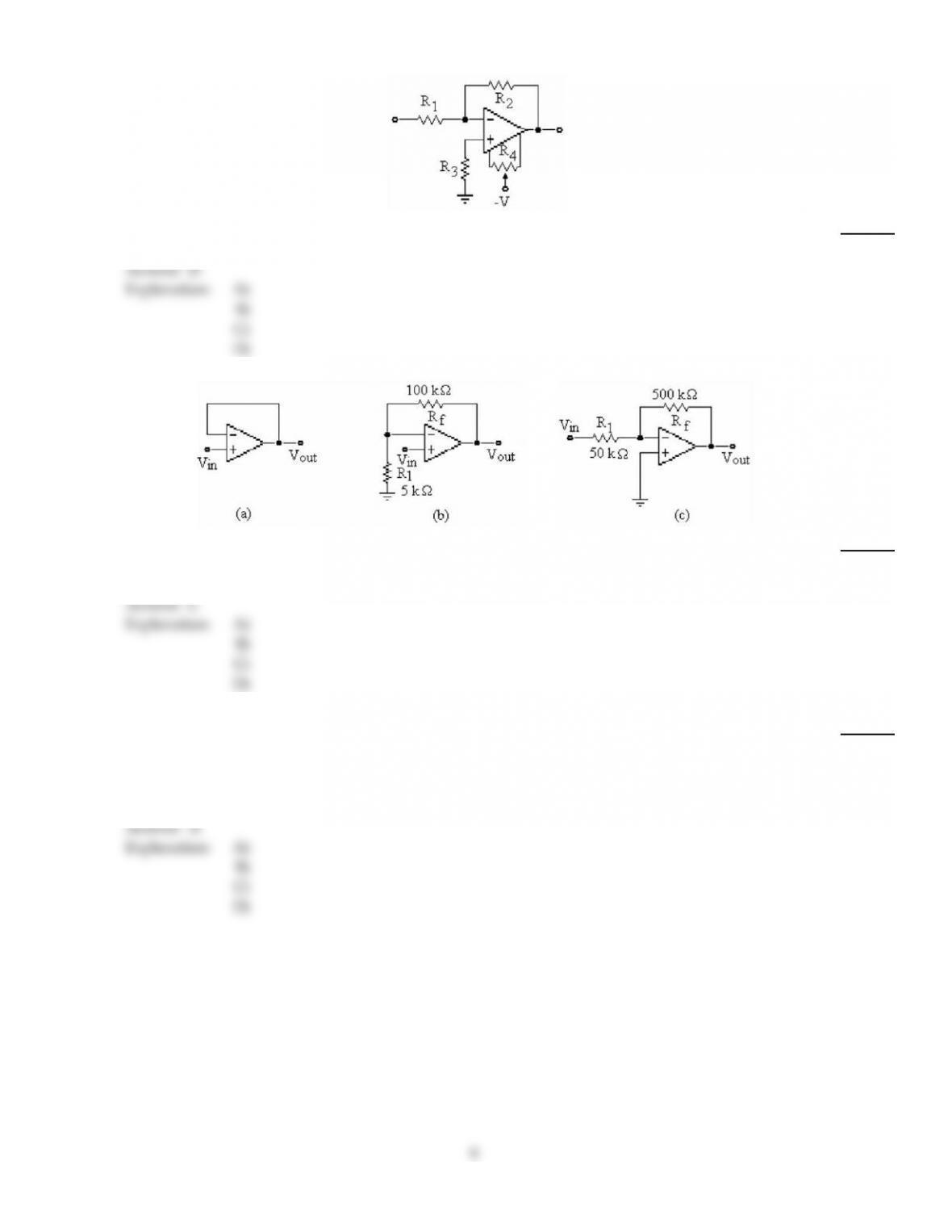
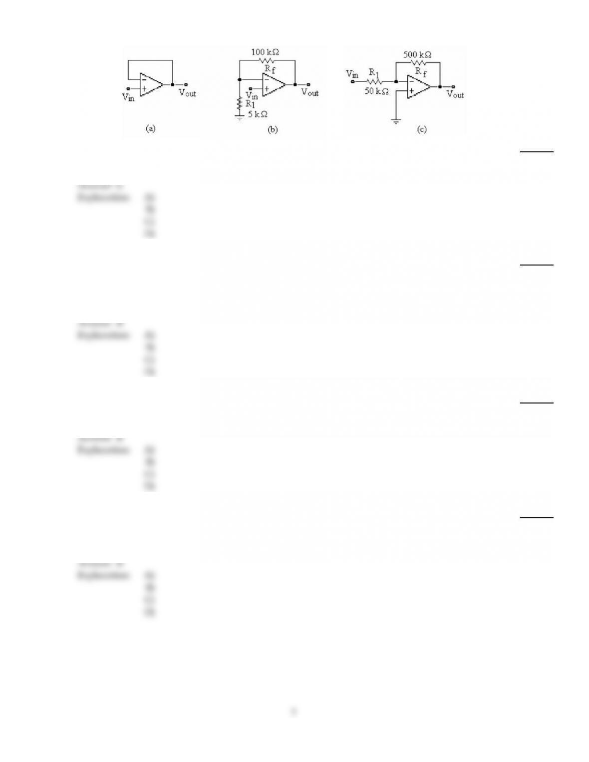
Refer to the figure above. Which circuit is a voltage follower?
1)
A)
(a)
B)
(b)
C)
(c)
D)
None of the above.
Answer:
A
Explanation:
A)
B)
C)
D)
2)
Refer to (b) in the figure above. If this circuit has a Vin = 0.7, Vout would be
2)
A)
–14.7 V.
B)
14 V.
C)
0 V.
D)
14.7 V.
Answer:
D
Explanation:
A)
B)
C)
D)
3)
Which op–amp parameter is dependent upon the high frequency response of the amplifier stages
inside the op–amp?
3)
A)
Input offset voltage
B)
Short–circuit output current
C)
Input bias current
D)
Slew rate
Answer:
D
Explanation:
A)
B)
C)
D)
1
4)
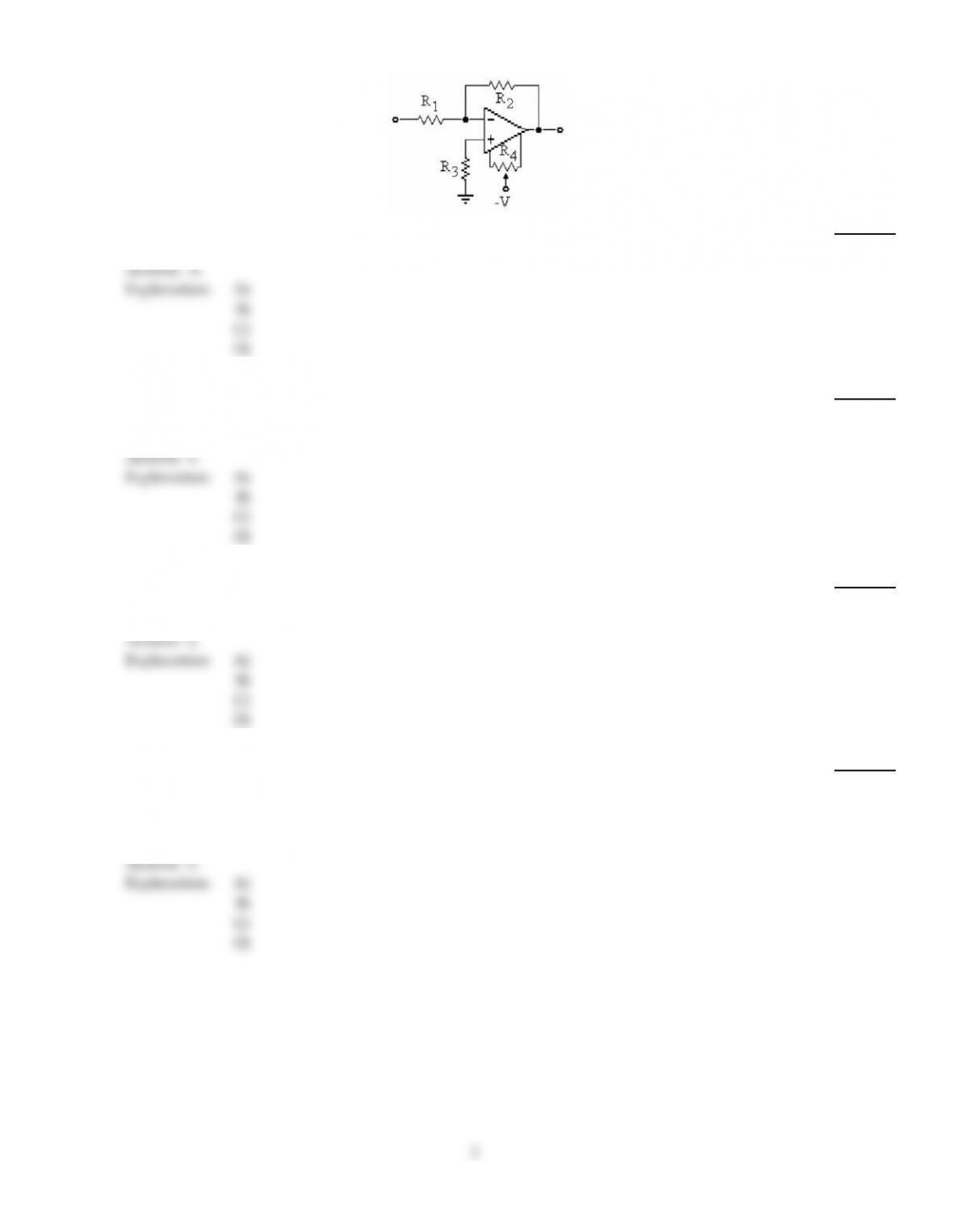
Refer to the figure above. Which components are used for offset voltage compensation?
4)
A)
R4
B)
R2
C)
R3
D)
R1 and R2
Answer:
A
Explanation:
A)
B)
C)
D)
5)
For a given op–amp, which of these is constant?
5)
A)
fC(CL)
B)
Feedback voltage
C)
AOL fc(OL)
D)
AOL
Answer:
C
Explanation:
A)
B)
C)
D)
6)
The op–amp can amplify
6)
A)
ac signals only.
B)
dc signals only.
C)
both ac and dc signals.
D)
neither ac nor dc signals.
Answer:
C
Explanation:
A)
B)
C)
D)
7)
The typical input stage of an op–amp has a(n)
7)
A)
emitter follower.
B)
push–pull circuit.
C)
two–input differential amplifier.
D)
single–ended input and differential output.
Answer:
C
Explanation:
A)
B)
C)
D)
2

8)
What type of input is provided to an op–amp for slew–rate measurement?
8)
A)
Sinusoidal voltage
B)
Step input voltage
C)
Triangle waveform
D)
Constant dc voltage
Answer:
B
Explanation:
A)
B)
C)
D)
9)
The ideal op–amp has
9)
A)
infinite input impedance and zero output impedance.
B)
infinite output impedance and zero input impedance.
C)
infinite voltage gain and infinite bandwidth.
D)
Both A and C.
Answer:
D
Explanation:
A)
B)
C)
D)
10)
The input offset current is
10)
A)
not related to the input bias currents.
B)
the difference between the input bias currents.
C)
less than the input offset voltage.
D)
unimportant when a base resistor is used.
Answer:
B
Explanation:
A)
B)
C)
D)
11)
The closed–loop input impedance in a noninverting amplifier is
11)
A)
sometimes less than the open–loop input impedance.
B)
much greater than the open–loop input impedance.
C)
ideally zero.
D)
equal to the open–loop input impedance.
Answer:
B
Explanation:
A)
B)
C)
D)
3
12)
The open–loop voltage gain (Aol) of an op–amp is the
12)
A)
same as Acm.
B)
external voltage gain the device is capable of.
C)
internal voltage gain the device is capable of.
D)
most controlled parameter.
Answer:
C
Explanation:
A)
B)
C)
D)
13)
Refer to the figure above. Which components are used for bias current compensation?
13)
A)
R2
B)
R3
C)
R4
D)
R1 and R2
Answer:
B
Explanation:
A)
B)
C)
D)
14)
With both inputs grounded, the only offset that produces an error is the
14)
A)
input short circuit current.
B)
input offset current.
C)
input offset voltage.
D)
input bias current.
Answer:
C
Explanation:
A)
B)
C)
D)
15)
What is the value of compensating resistor needed for a noninverting op–amp circuit using 10 k
resistors for both RI and RF?
15)
A)
100 k
B)
10 k
C)
5 k
D)
20 k
Answer:
C
Explanation:
A)
B)
C)
D)
4
16)
Refer to the figure above. Which circuit has an input impedance of about 5 k?
16)
A)
(a)
B)
(b)
C)
(c)
D)
None of the above.
Answer:
D
Explanation:
A)
B)
C)
D)
17)
The common–mode signal is applied to
17)
A)
the noninverting input.
B)
the inverting input.
C)
both inputs.
D)
None of the above.
Answer:
C
Explanation:
A)
B)
C)
D)
18)
Refer to (c) in the figure above. If an amplifier with an input impedance of 12 k and the same
voltage gain is needed, the new value of R1 would be ________ and the new value of Rf would be
________.
18)
A)
12 k, 108 k
B)
13.3 k, 120 k
C)
10 k, 100 k
D)
12 k, 120 k
Answer:
D
Explanation:
A)
B)
C)
D)
5
19)
Refer to the figure above. Which components are used to set input impedance and voltage gain?
19)
A)
R3 and R4
B)
R4
C)
R3
D)
R1 and R2
Answer:
D
Explanation:
A)
B)
C)
D)
20)
Refer to the figure above. Which circuit is the inverting amplifier?
20)
A)
(a)
B)
(b)
C)
(c)
D)
None of the above.
Answer:
C
Explanation:
A)
B)
C)
D)
21)
An inverting amplifier with a gain of –8 means that
21)
A)
the signal amplitude is increased by a factor of 8 with a 180° phase shift.
B)
the signal is attenuated by a factor of 8.
C)
the stage reduces the signal by a factor of 8 from input to output.
D)
ac and dc signals are increased by a factor of 8 with no phase shift.
Answer:
A
Explanation:
A)
B)
C)
D)
6
22)
Refer to the figure above. Which circuit has a voltage gain of 10?
22)
A)
(a)
B)
(b)
C)
(c)
D)
None of the above.
Answer:
C
Explanation:
A)
B)
C)
D)
23)
The input offset current equals the
23)
A)
difference between two base–emitter voltages.
B)
difference between two base currents.
C)
average of two base currents.
D)
collector current divided by current gain.
Answer:
B
Explanation:
A)
B)
C)
D)
24)
The loop gain AOLB
24)
A)
is between 0 and 1.
B)
is usually much greater than 1.
C)
may not equal 1.
D)
is usually much smaller than 1.
Answer:
B
Explanation:
A)
B)
C)
D)
25)
A voltage follower amplifier comes to you for service. With a sine wave input of 1 V, the output is
squared off at approximately 30 V peak–to–peak. The most likely problem is
25)
A)
the output is shorted to ground.
B)
open feedback loop.
C)
no dc supply voltage.
D)
the input is shorted to ground.
Answer:
B
Explanation:
A)
B)
C)
D)
7