Page 1 of 17
Power Supply
Shashidharan p, Former HOD, Dept. of Physics, Vartak College
The alternating voltage is given by V = Vmsinωt = Vmsinθ where θ = ωt = 2πft is the angular
frequency, t is the time and f is the frequency.
The average value over a complete cycle is given by
Vavg =0ꭍ2πVmsinθdѳ / 0ꭍ2πdѳ = Vm0ꭍ2πsinθdѳ / 2π = Vm/2π[-cosθ]02π = 0
Similarly Iavg over a complete cycle will also be equal to zero.
However the average value calculated over half the period works out to be
Vavg =0ꭍπVmsinθdѳ / 0ꭍπdѳ = Vm0ꭍπsinθdѳ / π = Vm/π[-cosθ]0π = 2Vm/π
Similarly Iavg over a half the cycle works out be 2Im/π.
The RMS value or effective value of AC is that value of DC, which would produce the same amount
of heat as would be produced by the AC, in a given resistor in the same time. Note: All measuring
instruments except true RMS meters have their scale calibrated for the RMS value of a pure sine wave.
Let the AC be represented by Iac = Imsinωt = Imsinθ where θ = ωt. If it flows through a resistor R for a
small interval of time dt, the energy dissipated in the form of heat in time dt is
dEac = Im2sin2 θ R dѳ
Hence the average energy dissipated in one complete cycle is
Eac = 0ꭍTdEac/0ꭍTdt = 0ꭍ2π Im2Rsin2θdѳ / 0ꭍ2πdѳ = (Im2R/2π)0ꭍ2π[(1- cos2θ)/2]dѳ = (Im2R/2π)(1/2)[(θ-sin2θ)/2]02π
Therefore Eac = Im2R/2
If Idc is the DC that produces the same amount of heat in the same resistor, then
Idc2R = Im2R/2
Therefore Idc = Im/√2 = 0.707Im = Irms
Irms is defined as the virtual current or the effective current or RMS(Root Mean Squire) value of the
AC.
The ratio of the RMS value of AC to its avg value is defined as the Form Factor.
FF = Irms/Iavg = (Im/√2)/(2Im/π) = π/2√2 = 1.11
Power in AC circuit (Power Factor)
Consider a circuit in which the current leads the voltage by an angle ϕ. The instantaneous voltage and
current can be written as V = Vmsinωt and I = Imsin(ωt+ϕ) respectively.
The instantaneous power = VI = VmImsinωtsin(ωt+ϕ) = VmIm[sinωt(cosωt sinϕ +sinωtcosϕ)]
= VmIm[sin2ωtcosϕ)+ (sin2ωt/2) sinϕ]
The average power over a complete cycle is
Pavg = 0ꭍTVIdt/0ꭍTdt = (VmIm/T)[ 0ꭍT sin2ωtcosϕ dt)+ (0ꭍT sin2ωt/2) sinϕ dt]
= (VmIm/T)[ cosϕ 0ꭍT (1-cos2ωt)/2dt+ sinϕ /20ꭍT sin2ωtdt]
= (VmIm/T)( cosϕ /2) [ (t-sin2ωt/2ω)]0T+ (VmIm/T)( sinθ/2)[–cos2ωt/2ω]0T
= VmImcosϕ /2 = (Vm/√2) (Im/√2)cosϕ = VrmsIrmscosϕ
The quantity cosθ is called power factor.
Any circuit with L, C and R, cosϕ = R/√ (R2 + (XL~XC)2).
The average power Pavg is called True Power and VrmsIrms is called apparent power.
Therefore Power Factor = True Power / Apparent Power.
For a purely inductive or capacitive circuit the voltage or current is in quadrature.
Therefore ϕ = π/2 or cosϕ = 0. Hence Pavg is zero. Therefore power in a purely inductive or capacitive
load is called wattles power.
Page 2 of 17
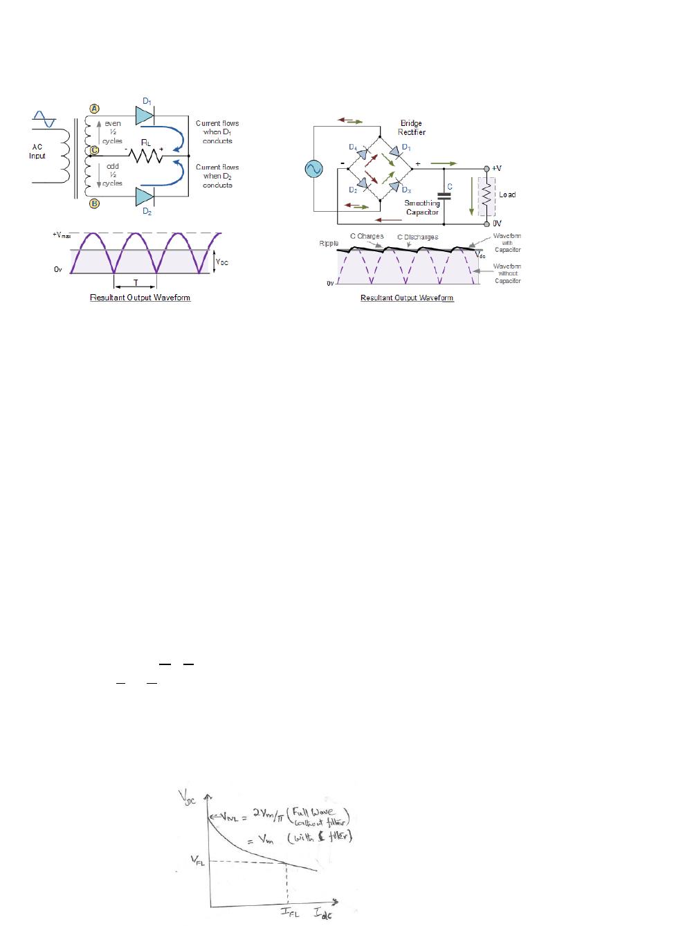
A Full Wave Rectifier is a circuit, which converts an ac voltage into a pulsating dc voltage using both
half cycles of the applied ac voltage. There exist two methods by which an AC can be converted into a
DC. 1) Centre tapped transformer type (Fig.1) and 2) Bridge rectifier type (Fig.1a). In a centre tapped
transformer for a required voltage the secondary winding has to be double than that of the transformer
used in a bridge rectifier type, while the count of diodes is vice-versa.
Fig.1 Fig.1a
Assuming an ideal diode, the current equation can be written as
I1 = Imsinωt for 0 ≤ θ ≤ π
= 0 for π ≤ θ ≤ 2π
I2 = 0 for 0 ≤ θ ≤ π
= Imsinωt for π ≤ θ ≤ 2π where Im = Vm/(RL + rf), RL is the load and rf is the diode resistance.
Since the current in each half cycle is identical, the avg or DC value is Idc = 2Im/π. Similarly the DC
voltage is Vdc = Idc* RL = 2Im/π* RL. Therefore the average power Pdc = Vdc* Idc = 4Im2/π2* RL.
IRMS = [0ꭍπ Im2sin2θdѳ / 0ꭍπdѳ]½ = (Im/√π)[0ꭍπ(1– cos2θ)/2dѳ]½ = (Im/√2√π){[θ-sin2θ]0π}½ = Im/√2.
Pac = IRMS2*(RL + rf) = Im2/2*(RL + rf)
Therefore the efficiency η = Pdc/Pac = (4Im2/π2* RL)/( Im2/2*(RL + rf)) = 8 RL/ π2(RL + rf)
= 0.812/(1+ rf/ RL)
Thus the theoretical maximum efficiency, when rf/ RL = 0, is 81.2%.
Voltage Regulation stands for how effectively the power supply can maintain its output voltage close
to the designed value with variation in output load current.
The percentage load (voltage) regulation is defined as
% load regulation = (VNL – VFL)/VFL*100 %
where VNL is called the No Load voltage, that is the output voltage when the current is zero or RL = ∞
and VFL is called Full Load voltage, that is the output voltage when load current is maximum.
For a full wave rectifier, Vdc = Idc* RL = 2Im/π* RL where Im = Vm/(RL + rf)
Therefore Vdc = 2Vm RL /π(RL + rf) = 2Vm /π[1– rf/(RL + rf)] = 2Vm /π – 2Vm rf /π(RL + rf)
= 2Vm /π – Idc rf
This shows that a full wave rectifier behaves like an ideal voltage source 2Vm /π with internal
resistance rf (Fig.1b).
Fig.1b
Page 3 of 17
Ripple Factor: is defined as the ratio of the AC component to the DC component.
It is given by γ = Iac/Idc.
Since the output of a rectifier is a fluctuating DC (Fig.1), it can be treated as the superposition of an
AC component over a DC component. The RMS current can be written as the vector sum of AC and
DC components. The effective RMS current can be written as Irms = (Idc2 + Iac2) ½.
Therefore Iac = (Irms2 – Idc2) ½
The ripple factor γ = Iac/Idc = √[(Irms/Idc)2 – 1]. Replacing Irms = Im/√2 and Idc = 2Im/π we get
γ = (π2/8 – 1) ½ = 0.482. This shows that AC component is lower than DC component.
Capacitor Filter: The rectified output of a full wave rectifier contains AC component. Hence it has to
be filtered out to obtain a ripple free DC output. The simplest method is to connect a capacitor to
bypass the AC to ground (Fig.1a). The output waveform is shown in Fig.1a. When the rectifier output
rises from 0 Volts to Vm Volts the capacitor is charged and also supplies current to the load RL. During
the next half of the output cycle the voltage falls to zero. During this period the capacitor supplies the
current required by the load leading the capacitor to discharge. Before the capacitor discharges fully
the next cycle will charge the capacitor. Let Tc be the charging time and Td be the discharge time.
Therefore we can write T = Tc + Td. where T is the time period of the pulsating DC at the output (the
time period of the input will be 2T).
Since discharge time Td is very large compared to charging time, we can write T ≈ Td. If f is the input
AC frequency, then T = 1/2f ≈ Td. If Vr(pp) is the peak-to-peak ripple voltage, then the charge stored
during charging time Tc will be Qcharge = Vr(pp)*C.
If Idc is the average current flowing, then the charge discharged in time Td will be Qdischarge = Idc*Td.
In the steady state the charge stored is same as charge discharged,
therefore Qcharge = Qdischarge, hence Vr(pp)*C = Idc*Td
Vr(pp) = Idc/2fC
Approximating the ripple voltage to a triangular voltage, the RMS value of ripple can be written as
Vr(rms) = Vr(pp)/2√3 = Idc/4√3fC = Vdc/4√3fCRL
Therefore the ripple factor γ = Vr(rms)/ Vdc = (4√3fCRL)-1 = 0.0028 for f = 50Hz, C = 1000 µF and RL = 1KΩ.
From Fig.1a, Vdc = Vm – Vr(pp)/2 = Vm – Idc/4fC = Vm – Vdc/4fCRL
Therefore Vm = Vdc(1 + 1/4fCRL)
Vdc = Vm(4fCRL)/(1 + 4fCRL)
Thus, if 4fCRL >> 1, then Vdc = Vm.
Power Supply: They generally classified into 1) Constant Voltage Source and 2) Constant Current
Source. A capacitor filter reduces the ripple by almost two orders of magnitude as compared to a
rectifier without filter. To further stabilise the DC output electronic circuits are used after filtering
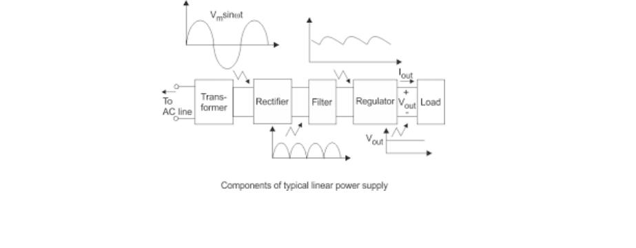
(Fig.2). These power supplies are called regulated power supplies.
Fig.2
A constant voltage source is a power source which provides a constant voltage to a load, even
despite changes and variance in load resistance (current).
Page 4 of 17
Zener Regulated Voltage Source
When the reverse bias voltage of a diode is increased beyond a critical value VBR the device starts to
conduct heavily and offers very little or no resistance. The reverse break down voltage VBR remains
constant for a very large range of reverse current. If the wattage (VBR*Irev) is maintained within the
capability of the device then it can operate without getting damaged. A diode operated in the break
down mode is called Zener diode or breakdown diode or avalanche diode. The breakdown voltage is
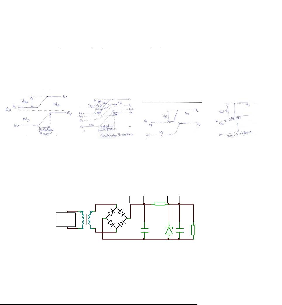
controlled by the doping concentration in the P and N regions of the diode (Fig.3 and Fig.3b). The
heavier the doping the lower is the breakdown voltage.
Avalanche breakdown and Zener breakdown are the two breakdown modes. In some cases it is
difficult to differentiate between the two. Generally Zener breakdown (Fig.3c) is observed when the
breakdown voltage is ≤ 5V and avalanche breakdown (Fig.3a) when VBR > 5V.
Fig.3 Fig.3a Fig.3b Fig.3c
The built-in-voltage or Forward Bias voltage VBi is given by VBi = (kT/e)*ln(NDNA/ni2) where k is
Boltzman constant, T is temperature in Kelvin, e is electronic charge, ND and NA are the donor and
acceptor concentrations and ni is the intrinsic carrier concentration (for Si at RT it is 1010 cm-3). A
simple voltage regulator uses the reverse breakdown mode of a Zener diode to maintain a steady
output voltage with varying currents through the load RL.
N1 N2
TR 2
1N1183 1N2804
Rz 180
RL 1k
10u
1m
AC
Mains
Vdc Vz
Fig.3d
Let Wz be the wattage of the zener diode (take it as 400 mW unless specified explicitly) and Vz be the
zener voltage. Hence the maximum current that can be passed through the zener without damaging it is
Izmax = Wz/Vz. Hence the voltage VRz = (Vdc – Vz) must be dropped across Rz. Usually the current Izmax
is derated by 50%. If more current has to be pumped through the zener, proper heat shunting should be
provided.
Electronically regulated power supply (Linear Voltage Regulator)
Simple series voltage regulator: A 9V unregulated DC source with a capacitor filter C (1000muF) is
regulated by a shunt regulator formed by Rz and zener diode Z1. The regulated, stable zener voltage
Vz is applied to the base of transistor Tr1 (Fig.4). The base-emitter voltage VBE of Tr1 will be between
0.6V to 0.7V. Therefore the output voltage of the regulated power supply will be Vout = Vz – VBE.
The fall in Vout due to increased demand for current will cause increase in VBE increasing ICE through
Tr1. The increased current through load will regulate output voltage Vout. A reduction in load current
will increase Vout reducing VBE which in turn reduces ICE causing VCE to increase, thus regulating Vout.
In this simple circuit regulation is not perfect.
Tr1 2N3053
Z1 1N3997
Rz 370
RL 1k
+
Vdc 9v
C 1m C1 100n
Unregulated
DC – Vdc
Vout
Tr1 2N3053
Z1 1N3997
Rz 370
RL 5
+
Vdc 9v
C 1m C1 100n
Tr2 2N3053
Rol 700m
Unregulated
DC – Vdc Vout
Z2 1N3822
D1 1N1183
Th 2N1595
Rov1 22
P1 100
Rov2 22 Rg 220
Rlimit 5
Vout – 5V
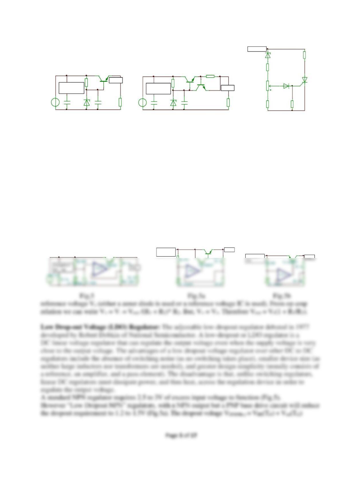
Fig.4 Fig.4a Fig.4b
Overload (current) Protection: The simple circuit in Fig.4 do not have overload protection which
can lead to circuit damage. The circuit in Fig.4a has a over-load protection. As the load current
increase above 1A, the transistor Tr2 will switch on due to overload sensing resistor Rol (0.7Ω)there by
switching off Tr1 (The collector current of Tr2 will reduce base current of Tr1).
Over Voltage Protection: The unregulated input to the regulator is much higher than the regulated
output many regulators incorporate over voltage protection. A simple protection circuit generally
called as “Crowbar” is shown in Fig.4b. The zener voltage of Z2 is lower than Vout so that the
difference is across Rov1, P1 and Rov2. Potentiometer P1 is adjusted so that the diode D1 is out of
conduction. If Vout increases, the increase in voltage will appear across Rov1, P1 and Rov2 forcing diode
D1 into conduction switching on the thyristor Th. The resistor Rlimit will limit the current through the
thyristor, but will be large enough to activate the overload function of the regulator thereby switching
off the series transistor Tr1. When voltage falls to zero the thyristor will switch off and Vout will appear
across the load RL.
Series Regulator using Op-Amp: In this type, the series element Tr1 is controlled by an op-amp
(Fig.5). The output voltage is sensed using potential divider network and compared with a constant
Vout
Unregulated
Vdc
Unregulated