**BY DR. RAVI PANWAR @IIIT JABALPUR, INDIA
CONCEPT OF NEGATIVE RESISTANCE
Negative resistance: a very important property of active two terminal microwave devices.
The real part of the impedance is negative over a range of frequencies.
Positive resistance
Negative Resistance
1. In a positive resistance, the
current through the resistance
and the voltage across it are in
phase.
1. In a negative resistance, the current
through the resistance and the
voltage across it are out of phase by
180◦
2. The voltage drop across a
positive resistance is +ve.
2. Voltage drop: -ve.
3. A power dissipation of I2R will
take place in the resistor.
3. A power generation of (-I2R) by
power supply will take place.
4. Positive resistances absorb
power (passive devices)
4. Negative resistances generate power
(active devices)
GUNN DIODE/ TRANSFERRED ELECTRON DEVICE (TED)
Negative resistance device: Exhibits a negative differential resistance that can be used to
generate microwave power directly from a DC source, when properly biased.
Invented by John Battiscombe Gunn (J. B. Gunn) (1963).
Also known as Transferred Electron Device (TED) and are low noise device at microwave
frequencies.
GUNN discovered periodic fluctuations of current passing through the n-type gallium
arsenide (GaAs) specimen, when the applied voltage exceeded a certain threshold value.
He showed that one could generate microwaves by applying a steady voltage across a chip of
n-type GaAs semiconductor.
Similar effects were also observed for compound semiconductors like GaAs, Indium
phosphate (InP), Cadmium Telluride (CdTe), and other semiconductors (CdTe, TnSb, InAs,
etc.)
Basic Construction of GUNN Diode
It consists of only n-type semiconductor, in which electrons are the majority charge carriers.
The material used to manufacture Gunn diodes should necessarily be of n-type as the
transferred electron effect holds good only for electrons and not for the holes.
**BY DR. RAVI PANWAR @IIIT JABALPUR, INDIA
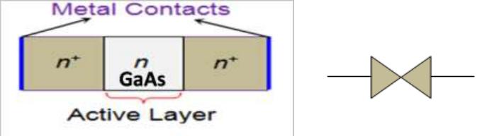
Here we don’t have any junction. There is a n-type GaAs crystal diode (active n-layer)
with regions of high doping (highly doped n+ regions) as shown in Figure below.
Although there is no junction (like PN junction), the GUNN diodes are named as diodes,
because of two metallic end contacts (as cathode and anode) in a single bulk semiconductor
such as n-GaAs. These metal contacts are provided at either end of the Gunn diode to
facilitate biasing.
General manufacturing procedure involves growing an epitaxial layer on a degenerate n+
substrate to form three n-type semiconductor layers (as shown in Figure), wherein the
extreme layers are heavily doped when compared to the middle, active layer.
Internal structure and circuit symbol of GUNN Diode
Since GaAs is a poor conductor, so considerable heat is generated in the device. So, a heat
sink may be provided so that this heat can come out the device.
Generally, semiconductors have a valence band, conduction band, and a band gap. But
some semiconductors like Gallium Arsenide (GaAs), Indium Phosphide (InP), and
Cadmium Telluride (CdTe), they have closely spaced sub bands (or closely spaced
multiple energy valleys) in the conduction band.
GUNN diodes can be made from the materials which consist of multiple, initially-empty,
closely-spaced energy valleys in their conduction band like Gallium Arsenide (GaAs),
Indium Phosphide (InP), Gallium Nitride (GaN), Cadmium Telluride (CdTe), Cadmium
Sulfide (CdS), Indium Arsenide (InAs), Indium Antimonide (InSb), and Zinc Selenide
(ZnSe).
**BY DR. RAVI PANWAR @IIIT JABALPUR, INDIA
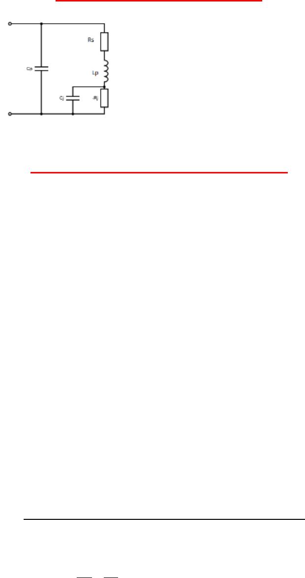
Equivalent Circuit of GUNN Diode
Cj, -Rj– Junction resistance and
inductance
Rs– Lead, ohmic contacts, bulk
resistance of diode
Cp, Lp– Package resistance and
inductance
Negative resistance: typically -5
to –20 Ω.
GUNN’s Effect/Transferred Electron Effect
The operation of GUNN diode is based on the GUNN’s effect (also known as Transferred
electron effect).
On applying a DC voltage across the terminals of the Gunn diode, an electric field is
generated in the sample with current I, most of which appears across the central active
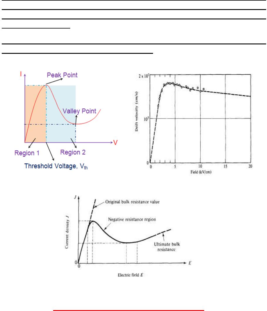
region. The typical VI characteristics of GaAs semiconductor are shown in Figure below.
At initial stages, the conduction increases due to the movement of electrons from the valence
band into the lower valley of the conduction band.
From GUNN’s observation, there is a threshold limit of electric field (or applied bias
voltage). At threshold voltage, E field is 3.2 KV/cm for GaAs. The threshold value of E
field for InP is 10.5 KV/cm.
Before, threshold limit, it shows Ohm’s law behavior (i.e., more voltage means more
current). It has been observed that, the carrier drift velocity (or current) is linearly increased
(following from zero to a maximum), when the electric field is varied from zero to a
threshold value.
But when the electric field is beyond the threshold value of 3.2 KV/cm for the n-type GaAs,
the current became a fluctuating function of time. The transferred electron become pre-
dominant, and increase in bias voltage results in the decrease in the current/drift velocity.
As a result the diode is said to exhibit a negative differential resistance region (a region
spanning from Peak point to Valley Point) in the V-I characteristic curve. The
corresponding J-E plot is also shown in Fig. below.
dI dJ NEGATIVE RESISTANCE
dV dE
**BY DR. RAVI PANWAR @IIIT JABALPUR, INDIA
This differential negative resistance (or simply negative resistance) of the device is used for
making a microwave GUNN oscillator. When the negative resistance of the device is
compensated by the positive resistance of the external resistance circuit, sustained
oscillations takes place.
This effect is called GUNN’s Effect or transferred electron effect and thus the Gunn
diodes are also called Transferred Electron Devices.
V-I Characteristics of GUNN Diode
Drift velocity of electrons in n-type GaAs
versus electric field
J-E Characteristics of GUNN Diode
RIDLEY-WATKINS-HILSUM (RWH) THEORY
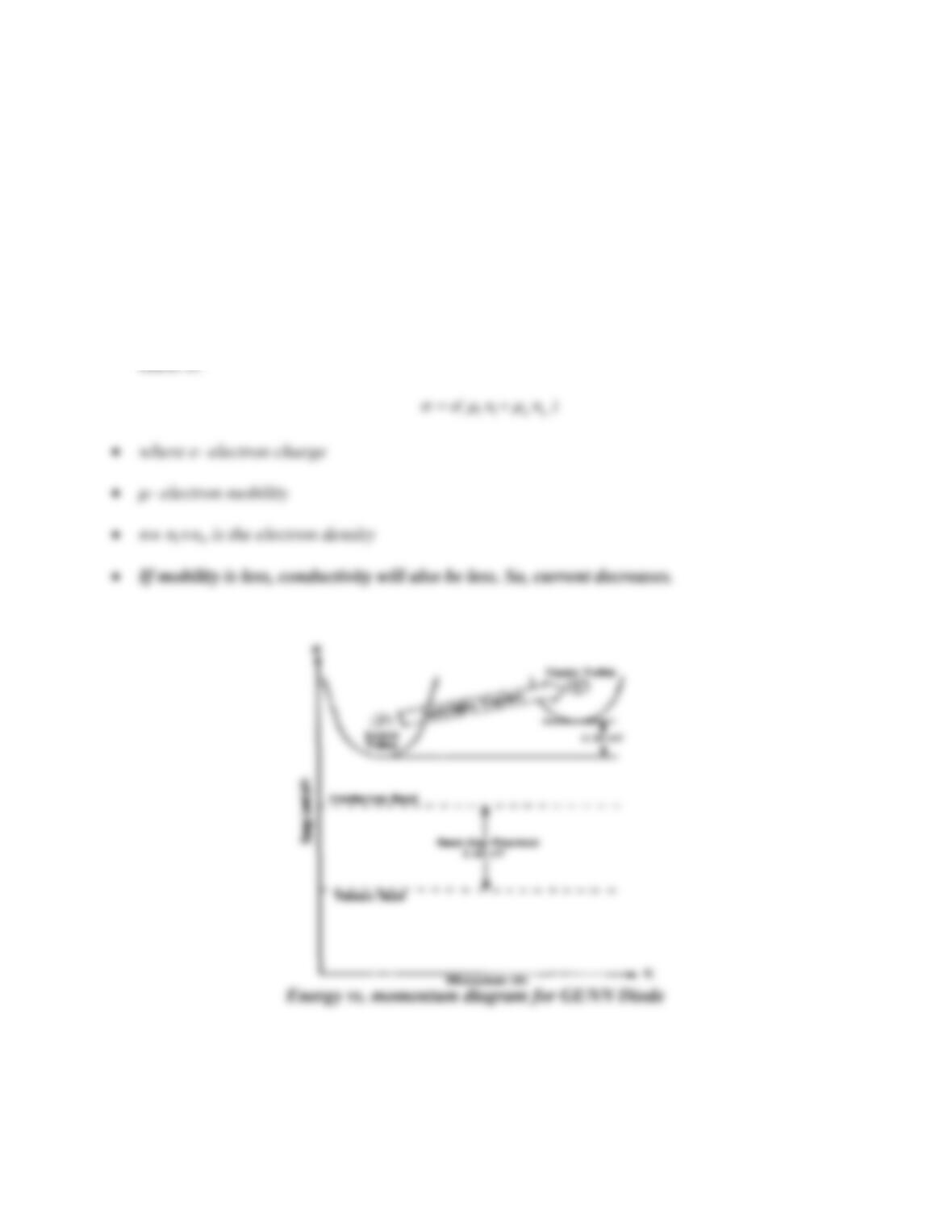
Used to explain the physics of the GUNN diode with the help of an Energy Vs. Momentum
diagram.
When a DC bias is applied across the material, an E field is produced.
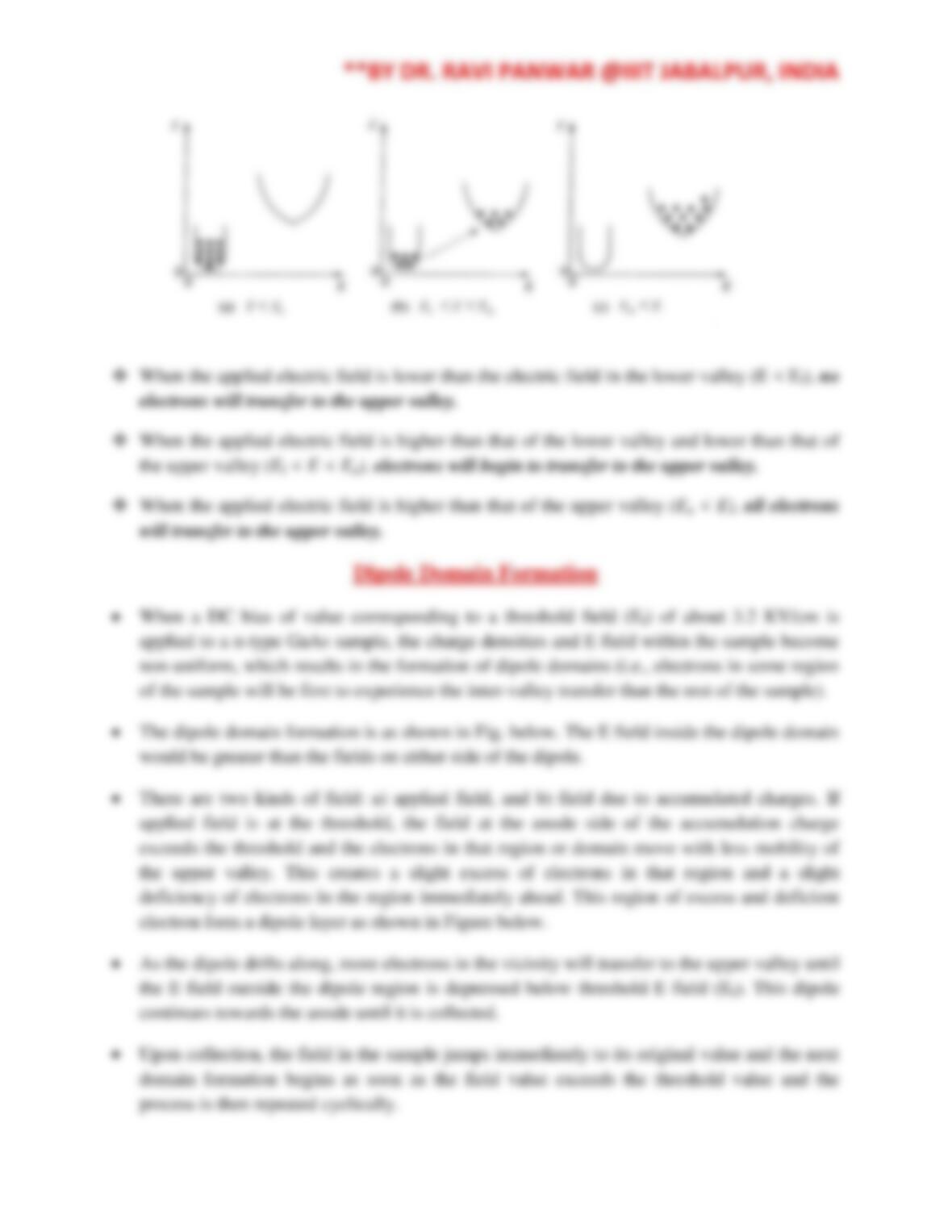
At lower E field, most of the electrons reside in the lower valley (because energy is small).
**BY DR. RAVI PANWAR @IIIT JABALPUR, INDIA
At higher E field (means when we apply more bias), most of the electrons will be
transferred to the higher energy (i.e., upper valley). Here electrons get energy from that
bias and so transferred to upper valley.
In higher valley, effective electron mass is larger.
So, the electron mobility is lower.
Conductivity is directly proportional to mobility (conductivity α Mobility)
If electron densities in the upper and lower valleys are nl and nu, the conductivity of n-type