Unlock document.
This document is partially blurred.
Unlock all pages and 1 million more documents.
Get Access
Exam
Name___________________________________
MULTIPLE CHOICE. Choose the one alternative that best completes the statement or answers the question.
1)
An E-MOSFET has values of VGSth = 2 V and ID(on) = 8 mA when VGS= 10 V. What is the value
of k for the device?
1)
A)
80
B)
0.000125
C)
0.0001
D)
Cannot be determined from the information given
Answer:
B
Explanation:
A)
B)
C)
D)
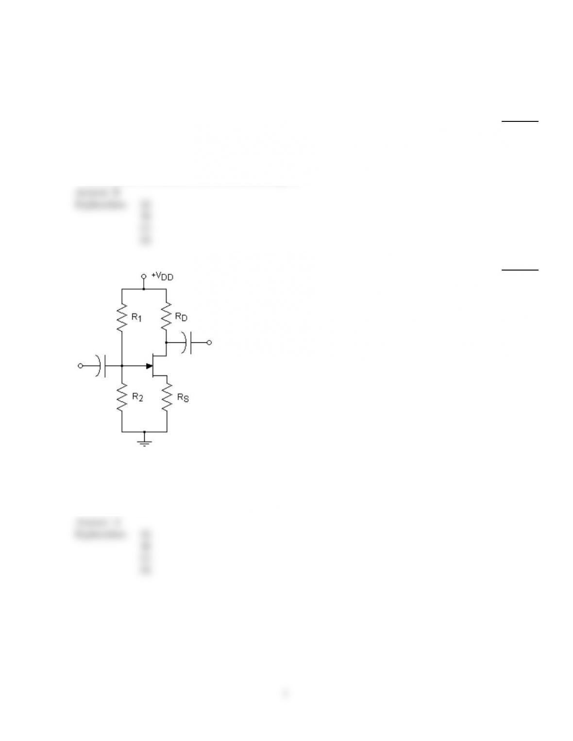
2)
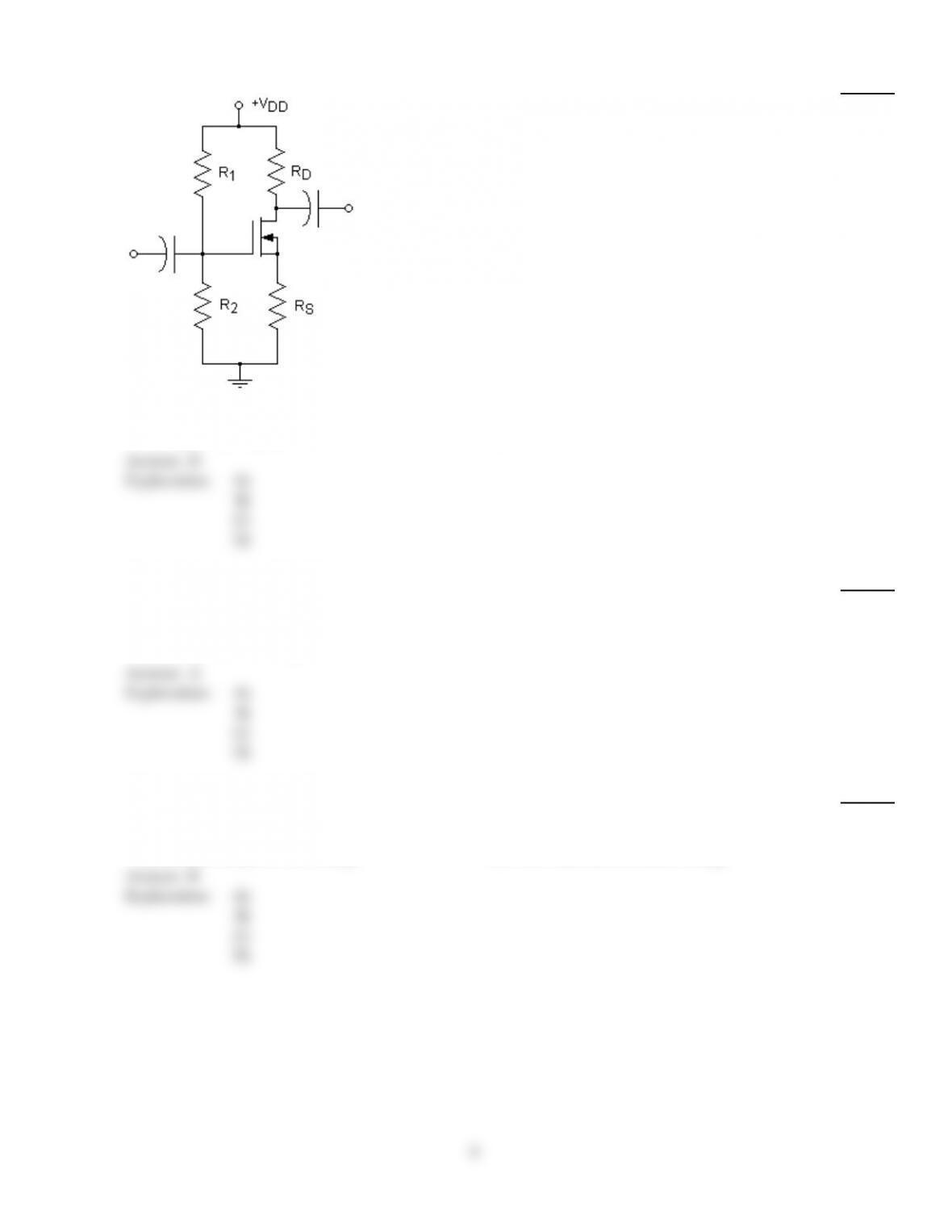
Which of the following is true for this circuit?
2)
A)
VG is measured between the gate and common.
B)
VG is equal to the voltage across RS.
C)
VG is measured between the gate and source terminals.
D)
VG is always close to +0.7 V.
Answer:
A
Explanation:
A)
B)
C)
D)
1
3)
This graphical solution represents ________.
3)
A)
fixed bias for an n-channel JFET
B)
self bias for an n-channel JFET
C)
voltage-divider bias for an n-channel JFET
D)
None of the above
Answer:
B
Explanation:
A)
B)
C)
D)
4)
Generally, it is a good design practice for linear amplifiers to choose the operating point that is
approximately ________.
4)
A)
near the origin
B)
in the center of the active region
C)
near the saturation region
D)
near the cut-off region
Answer:
B
Explanation:
A)
B)
C)
D)
2
5)
Which of the following equations properly characterize the value of VDS for this circuit?
5)
A)
VDS =VR1 +VR2 -IDRD+RS
B)
VDS =VDD -IDRD+RS
C)
VDS =VD-VS
D)
All of the above
Answer:
D
Explanation:
A)
B)
C)
D)
6)
Generally, it is good design practice for linear amplifiers to have operating points that close to
________.
6)
A)
the midpoint of the load line
B)
the cut-off region
C)
are close to saturation level
D)
None of the above
Answer:
A
Explanation:
A)
B)
C)
D)
7)
Which of the following biasing circuits can be used with E-MOSFETs?
7)
A)
zero bias
B)
current-source bias
C)
self bias
D)
drain-feedback bias
Answer:
D
Explanation:
A)
B)
C)
D)
3
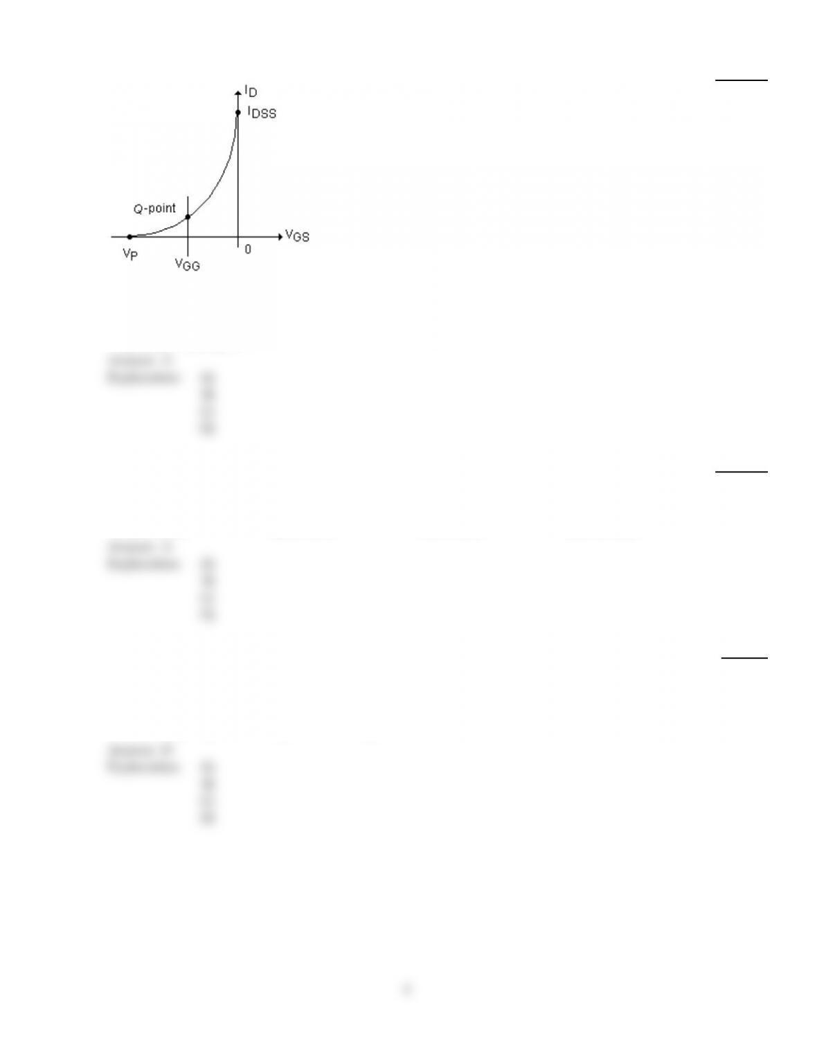
8)
This graphical solution represents ________.
8)
A)
fixed-bias configuration for an n-channel JFET.
B)
voltage-divider bias for an n-channel JFET
C)
self bias for an n-channel JFET
D)
None of the above
Answer:
A
Explanation:
A)
B)
C)
D)
9)
A JFET has the following ratings: VP= -2 V to -5 V and an IDSS = 4 mA. The device is being used
in a fixed-bias circuit with a gate supply voltage of VGG = 1 V. What is the difference between the
minimum and maximum values of ID values for the circuit?
9)
A)
1.56 mA
B)
2.6 mA
C)
3.6 mA
D)
1.65 mA
Answer:
A
Explanation:
A)
B)
C)
D)
10)
In a fixed-bias circuit for an n-channel JFET transistor the bias line ________.
10)
A)
is straight left and right parallel to the VGS axis
B)
is slanted and passes through origin
C)
is slanted and passing through the ID and the VGS axis on the positive side
D)
is straight up and down parallel to the ID axis
Answer:
D
Explanation:
A)
B)
C)
D)
4
11)
Calculate IDQ for this self-bias depletion mode MOSFET transistor amplifier if VGSQ = -4.625 V.
11)
A)
IDQ = 1.5 mA
B)
IDQ = 1.3 mA
C)
IDQ = 1.85 mA
D)
IDQ = 1.9 mA
Answer:
C
Explanation:
A)
B)
C)
D)
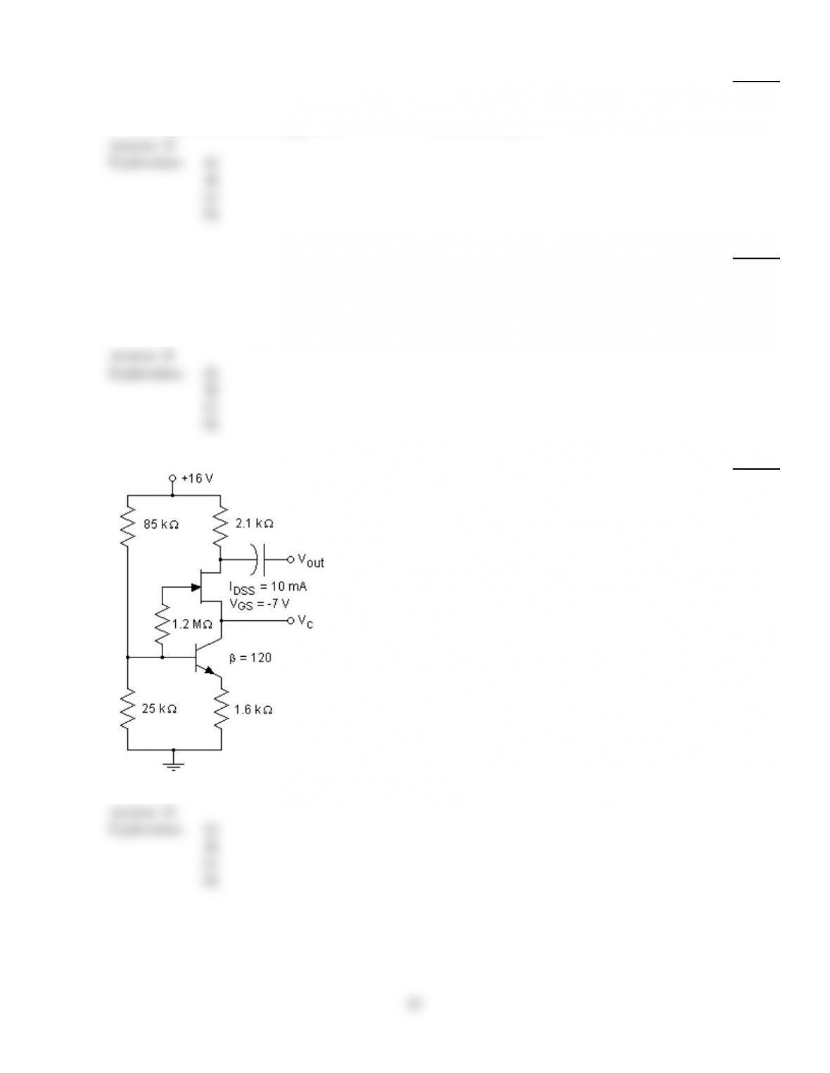
12)
Calculate the quiescent drain current for this circuit if VDS= 7.07 V.
12)
A)
IDQ = 2.97 mA
B)
IDQ = 2.5 mA
C)
IDQ = 3.3 mA
D)
IDQ = 3.37 mA
Answer:
C
Explanation:
A)
B)
C)
D)
5
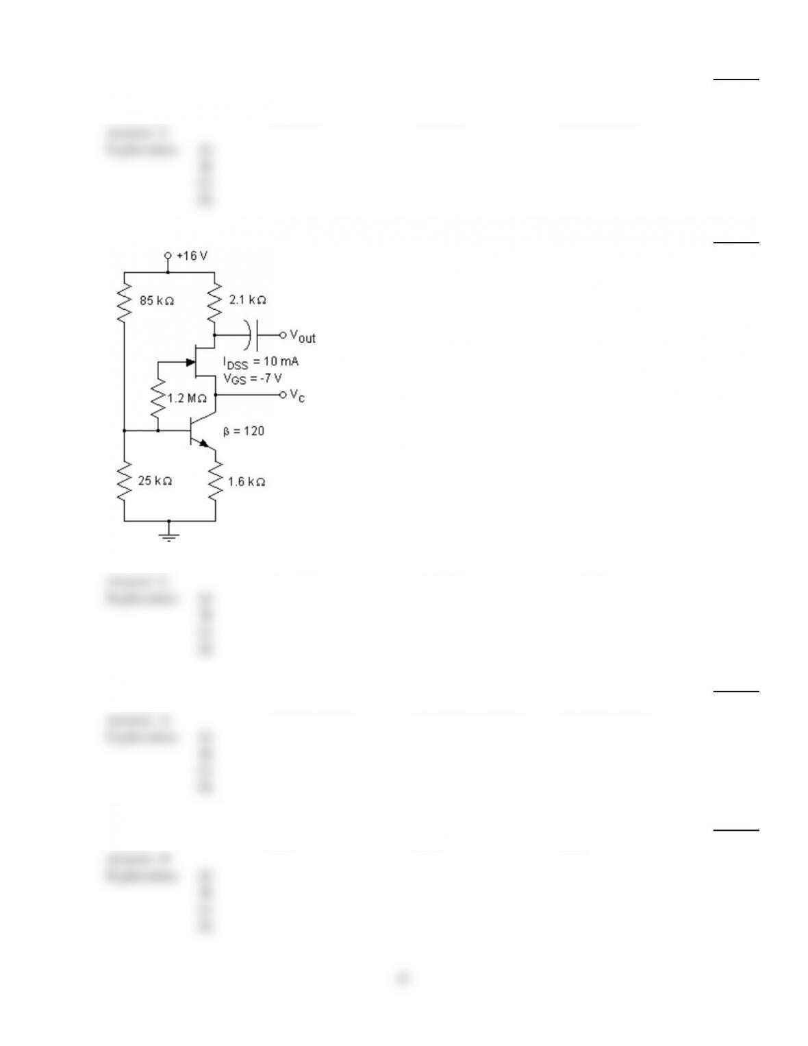
13)
Calculate the quiescent gate-to-source voltage for this circuit if IDQ = 2.8 mA.
13)
A)
VGSQ = -3.6 V
B)
VGSQ = 3.6 V
C)
VGSQ = 1.8 V
D)
VGSQ = -1.38 V
Answer:
D
Explanation:
A)
B)
C)
D)
14)
The simplest biasing arrangement for the n-channel JFET is ________.
14)
A)
fixed bias
B)
drain-feedback bias
C)
voltage-divider bias
D)
variable bias
Answer:
A
Explanation:
A)
B)
C)
D)
15)
The self-bias configuration develops the controlling gate-to-source voltage across a resistor
introduced in the ________.
15)
A)
gate leg
B)
drain leg
C)
source leg
D)
None of the above
Answer:
C
Explanation:
A)
B)
C)
D)
6
16)
Calculate the quiescent collector current for this circuit.
16)
A)
ICQ = 1.63 mA
B)
ICQ = 2.3 mA
C)
ICQ = 1.9 mA
D)
ICQ = 2.1 mA
Answer:
A
Explanation:
A)
B)
C)
D)
7
17)
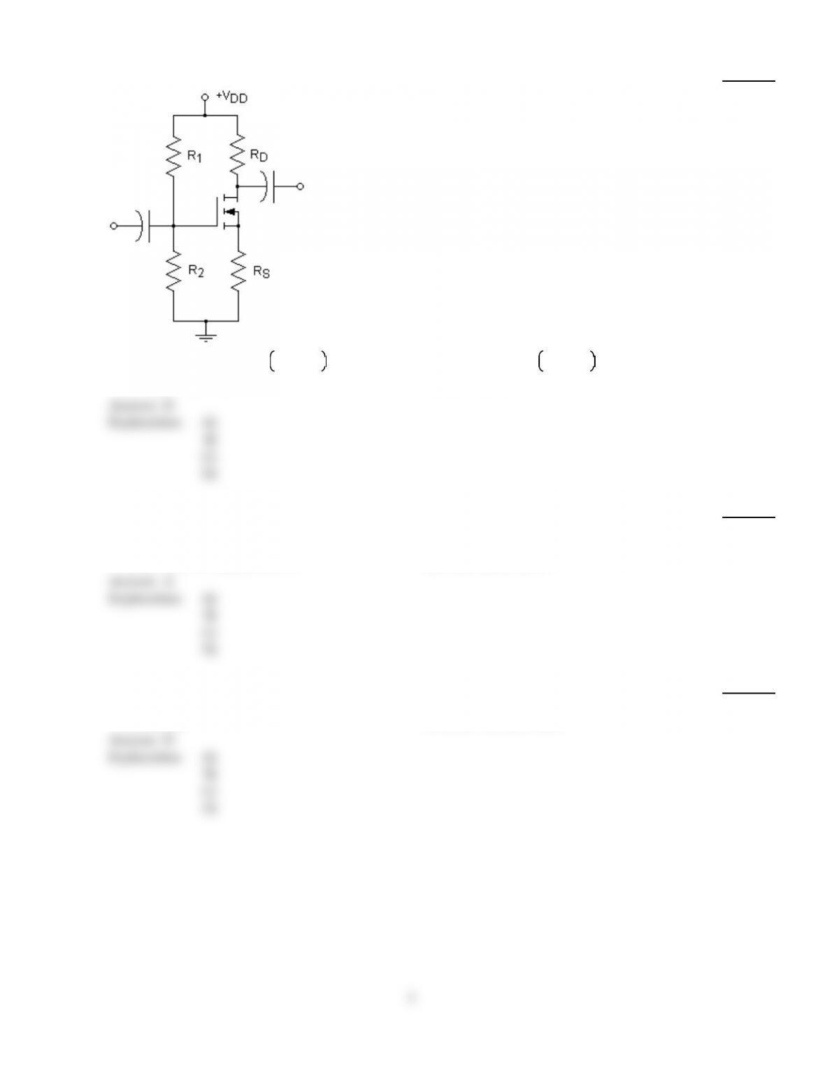
Which one of the following statements about this circuit is true?
17)
A)
VGS is equal to the voltage across RS.
B)
VGS is measured across R2.
C)
VGS is always close to +0.7 V.
D)
VGS is measured between the gate and source terminals.
Answer:
D
Explanation:
A)
B)
C)
D)
18)
A characteristic of voltage divider-bias in FET circuits is ________.
18)
A)
the current in both R1 and R2 is the same
B)
the gate current is zero
C)
the voltage drop across R2 is VGS
D)
A and C only
Answer:
D
Explanation:
A)
B)
C)
D)
8
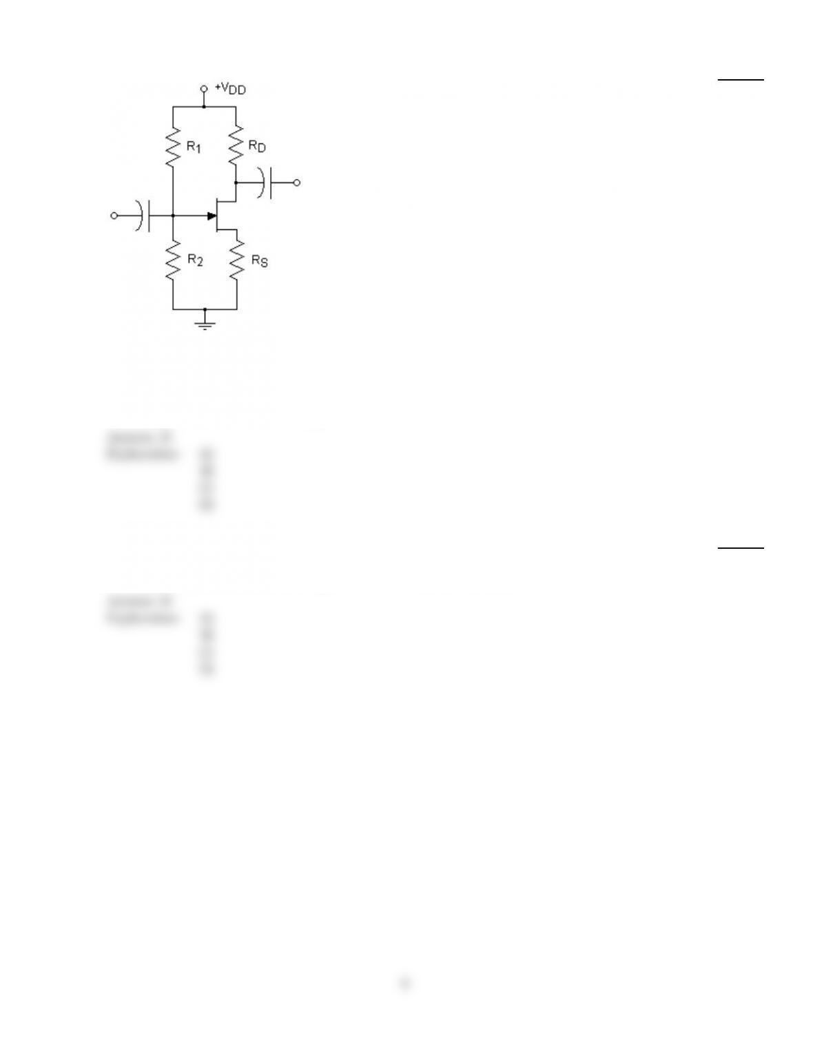
19)
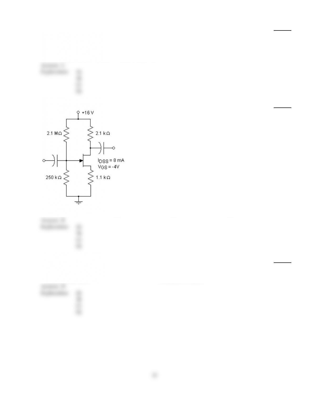
Which of the following expressions is correct for this circuit?
19)
A)
VGS=VG-ISRS
B)
VGS=VG-VS
C)
VGS=VG-IDRS
D)
All of the above
Answer:
D
Explanation:
A)
B)
C)
D)
20)
When using voltage divider-bias in FETamplifiers, increasing the size of the source resistor results
in ________.
20)
A)
lower quiescent IDvalues
B)
a larger value of drain current
C)
more positive of VGS
D)
All of the above
Answer:
A
Explanation:
A)
B)
C)
D)
21)
In the enhancement type of MOSFET the channel is formed when the gate-to-source voltage
________.
21)
A)
is less than the pinch-off voltage
B)
exceeds the threshold voltage
C)
exceeds the pinch-off voltage
D)
is less than the threshold voltage
Answer:
B
Explanation:
A)
B)
C)
D)
9
22)
A JFET can be biased in several different ways. The common method(s) of biasing an n-channel
JFET is(are) ________.
22)
A)
fixed-bias configuration
B)
self-bias configuration
C)
voltage-divider bias configuration
D)
All of the above
Answer:
D
Explanation:
A)
B)
C)
D)
23)
The primary difference between JFETs and depletion-type MOSFETs is ________.
23)
A)
depletion-type MOSFETs can have only positive of VGS
B)
depletion-type MOSFETs can have positive values of VGS and levels of ID that exceed IDSS
C)
JFETs can have positive values of VGS and levels of drain current that exceed IDSS
D)
JFETs can have only positive values of VGS
Answer:
B
Explanation:
A)
B)
C)
D)
24)
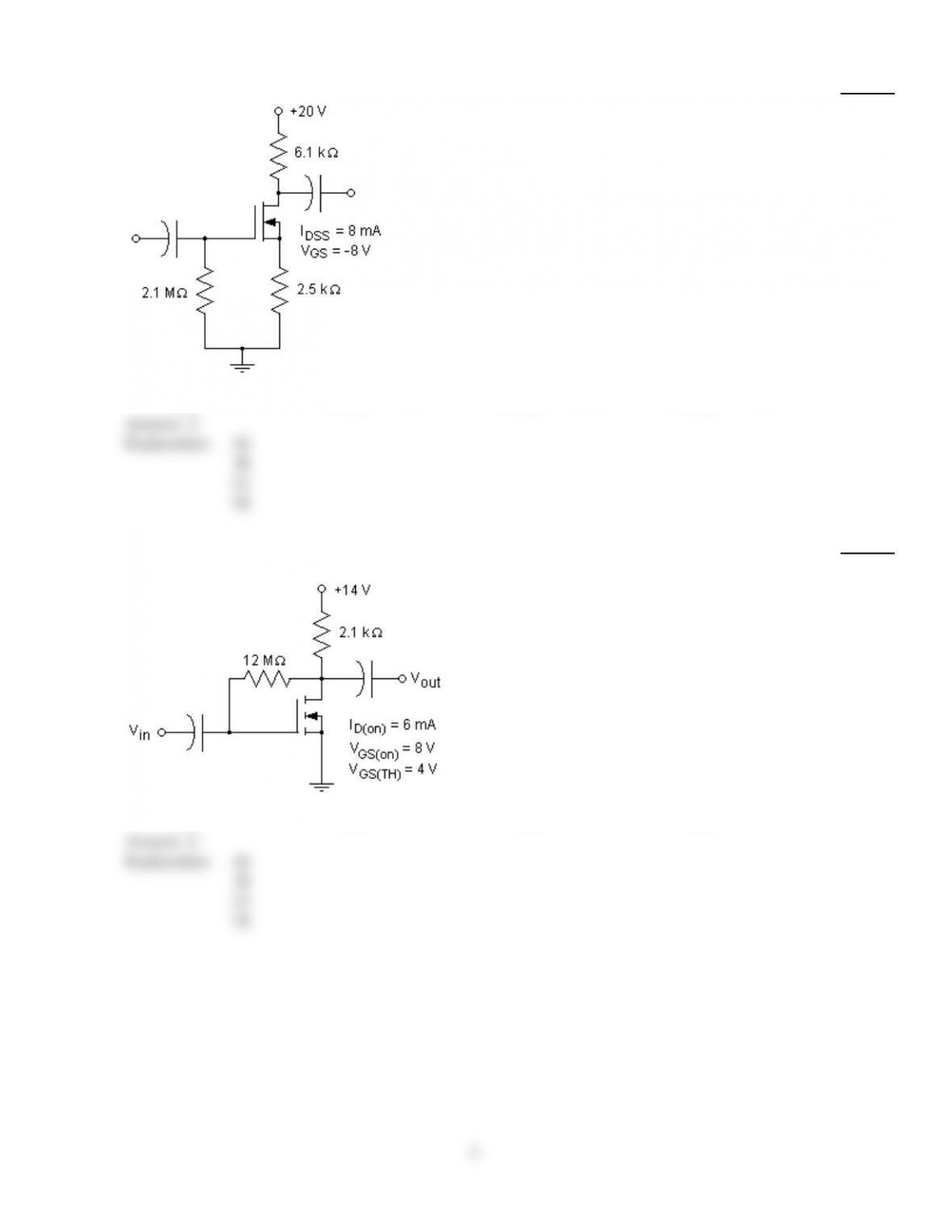
Calculate the voltage at the drain of the JFET in this combination network.
24)
A)
VD= 8.22 V
B)
VD= 4.14 V
C)
VD= 3.5 V
D)
VD= 12.58 V
Answer:
D
Explanation:
A)
B)
C)
D)
10
25)
An E-MOSFET has values of VDD = 14 V and RD= 2 k. . The device is being used in a circuit that
has a value of VGS= 6 V. What is the value of ID for the circuit?
25)
A)
1 mA
B)
0 mA
C)
4 mA
D)
13.33 mA
Answer:
C
Explanation:
A)
B)
C)
D)
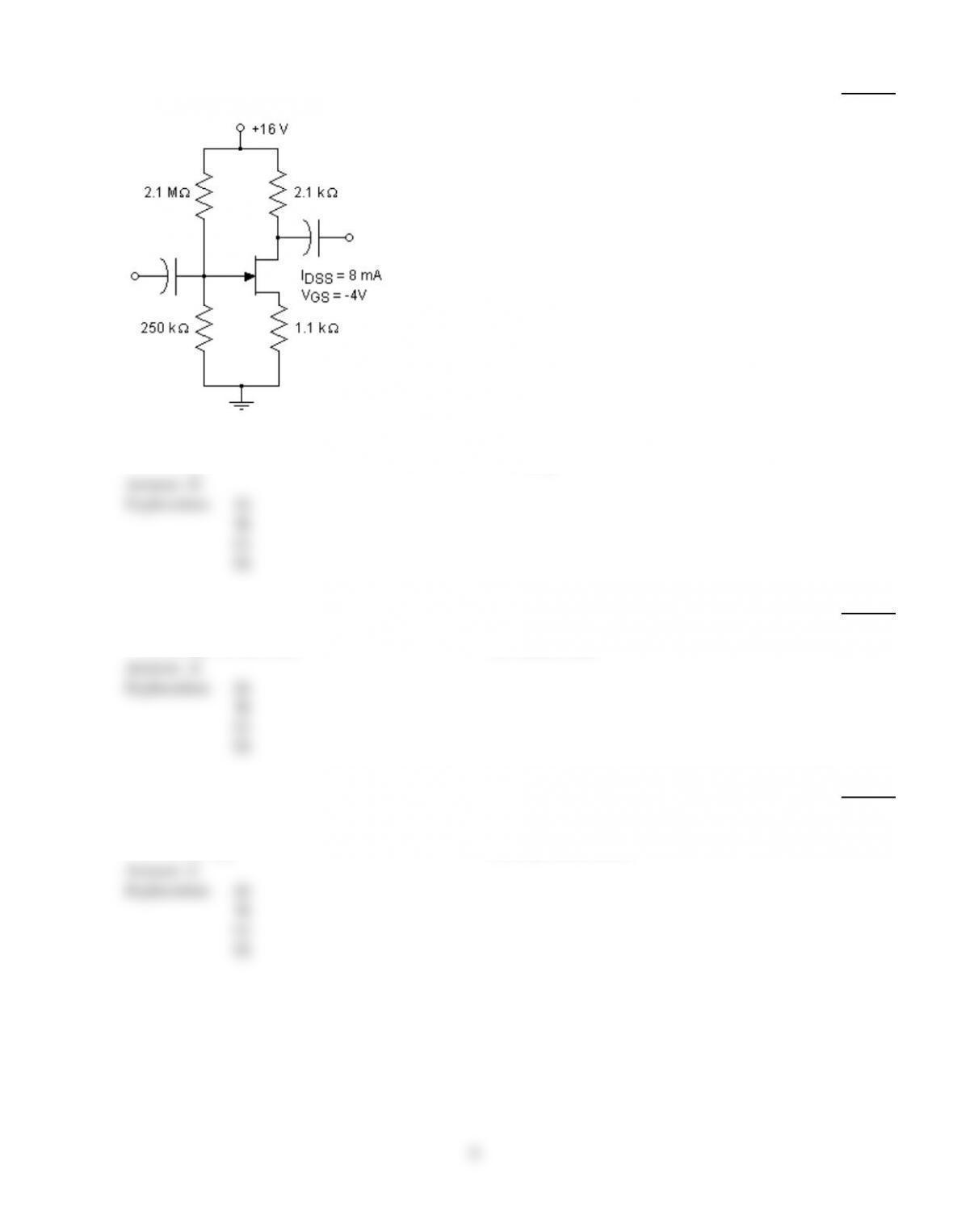
26)
Calculate the quiescent collector-to-emitter voltage for the BJT in this circuit if VGSQ = -3.65 V.
26)
A)
VCE = 7.78 V
B)
VCE = 5.11 V
C)
VCE = 4.34 V
D)
VCE = -4.14 V
Answer:
C
Explanation:
A)
B)
C)
D)
27)
________ biasing may be used with D-MOSFETs but not with JFETs.
27)
A)
Zero
B)
Gate-drain
C)
Current-source
D)
Gate-cutoff
Answer:
A
Explanation:
A)
B)
C)
D)
28)
The fixed-bias technique requires ________ power supplies.
28)
A)
1
B)
4
C)
3
D)
2
Answer:
D
Explanation:
A)
B)
C)
D)
11
29)
In a self-bias circuit for an n-channel JFET transistor the se1f-bias line ________.
29)
A)
is straight up and down parallel to the ID axis
B)
is slanted and passing through the ID and the VGS axis on the positive side
C)
is slanted and passes through origin
D)
is straight left and right parallel to the VGS axis
Answer:
C
Explanation:
A)
B)
C)
D)
30)
Calculate the drain-gate voltage for this voltage-divider bias circuit if IDQ = 2.8 mA .
30)
A)
VDG= 6.42 V
B)
VDG= 8.42 V
C)
VDG= 5.42 V
D)
VDG= 7.42 V
Answer:
B
Explanation:
A)
B)
C)
D)
31)
The analysis that we mostly work with is that of the n-channel device. For p-channel devices the
transfer curve employed is the ________ image and the defined current directions are ________.
31)
A)
identical; the same
B)
identical; reversed
C)
mirror; the same
D)
mirror; reversed
Answer:
D
Explanation:
A)
B)
C)
D)
12
32)
A popular arrangement for enhancement type MOSFET biasing is ________.
32)
A)
source-resistor bias
B)
fixed bias
C)
drain-feedback biasing
D)
All of the above
Answer:
C
Explanation:
A)
B)
C)
D)
33)
It is important to remember that when the JFET is used as a voltage variable resistor, which is one
of its practical applications, the voltage VDS is ________ VDS(max) and |VGS| is ________ |VP|.
33)
A)
very much greater than; very much less than
B)
very much less than; very much less than
C)
very much greater than; very much greater than
D)
very much less than; very much greater than
Answer:
B
Explanation:
A)
B)
C)
D)
13

Answer Key
Testname: C7
1)
B
2)
A
3)
B
4)
B
5)
D
6)
A
7)
D
8)
A
9)
A
10)
D
11)
C
12)
C
13)
D
14)
A
15)
C
16)
A
17)
D
18)
D
19)
D
20)
A
21)
B
22)
D
23)
B
24)
D
25)
C
26)
C
27)
A
28)
D
29)
C
30)
B
31)
D
32)
C
33)
B


